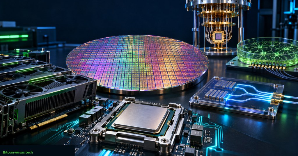
A video published October 24, 2026, by Bit by Bit Explained surveys 20 different computing engines, from familiar CPUs and GPUs to quantum chips, optical circuits and living-neuron systems. The categories reveal a practical shift: computing hardware is increasingly optimized for the kind of work being performed rather than measured by a universal speed score. A peer-reviewed October 23 study on optical neuromorphic computing offers a timely example of research moving beyond conventional digital arithmetic.
Bit by Bit Explained, “Every Processing Unit Explained in 20 Minutes,” published October 24, 2026. The overview introduces all 20 categories; its conceptual comparisons are not independent performance benchmarks. Credit: Bit by Bit Explained / YouTube.
The processors already handling everyday tasks
A central processing unit (CPU) handles flexible operating-system and application instructions, while a graphics processing unit (GPU) performs large numbers of parallel operations for rendering, scientific computing and AI. An accelerated processing unit (APU) integrates CPU and graphics capabilities on one chip. A physics processing unit (PPU) targets simulation of collisions and movement, although modern GPUs and CPUs also perform physics workloads. For architectural background, see BitcoinVersus.Tech’s CPU, GPU and NPU comparison.
A microcontroller unit (MCU) combines processing, memory and peripherals for embedded control; an image signal processor (ISP) transforms camera-sensor data into usable pictures. A security processor isolates sensitive operations such as key management. SPU is not a universal architecture label: historical systems have used it for specialized signal or synergistic processing units, so a specific implementation must be identified before comparing performance.
AI accelerators and configurable silicon
A neural processing unit (NPU) accelerates neural-network inference, commonly in phones and PCs. Google’s tensor processing unit (TPU) is a purpose-built AI application-specific integrated circuit (ASIC) using matrix-multiply arrays. A language processing unit (LPU), associated with Groq’s architecture, emphasizes deterministic, low-latency language-model inference. An ASIC more broadly hardwires a particular function; Bitcoin mining chips are one example. An FPGA can be reconfigured after fabrication, while a data processing unit (DPU) offloads infrastructure tasks such as networking, storage and security. See earlier coverage of AI chip choices and FPGA demand.
Google Cloud Tech, “Scaling AI with Google Cloud’s TPUs,” November 12, 2025. Official explanation of matrix engines, memory and TPU scaling; earlier educational footage, not October 2026 hardware news. Credit: Google Cloud Tech / YouTube.
Wafer-scale processors and quantum machines
A wafer-scale engine (WSE) keeps a vast processor fabric on a single wafer rather than dividing it into conventional dies. Cerebras lists 900,000 AI cores and four trillion transistors for its WSE-3 Turbo; its August 2026 CS-4 system combines three wafers. Those are manufacturer specifications, not proof of universal superiority over GPUs. The site’s Cerebras wafer-scale coverage explains deployment context. A quantum processing unit (QPU) manipulates qubits for certain quantum algorithms and experiments, but error correction and scale remain major obstacles. IBM’s quantum-system report describes the separate engineering path.
Cerebras, “Cerebras Supernova 2026,” August 21, 2026. Official presentation of CS-4 and WSE-3 Turbo; speed and efficiency comparisons are vendor claims rather than independent cross-platform benchmarks. Credit: Cerebras / YouTube.
Computing with photons, randomness and cells
Neuromorphic processors model brain-inspired spiking activity; BrainChip’s developer hardware is one commercial example. Photonic processors use optical signals for selected calculations. On October 23, researchers published SEPhIA, an electro-photonic spiking-network design reaching more than 90% accuracy in a simulated four-class classification task. The authors modeled experimentally informed device behavior; they did not report a fully fabricated, deployed classifier.
A thermodynamic sampling unit (TSU), as described by Extropic, uses transistor fluctuations to sample probability distributions; its manufacturer explicitly distinguishes sampling from ordinary deterministic processing. A biological processing unit instead couples cultured neurons with electrodes and software, exemplified by Cortical Labs’ CL1. Neuron cultures require controlled living conditions and raise distinct reproducibility and ethical questions; see BitcoinVersus.Tech’s biological computing coverage.
No single processor wins every workload
The 20 labels are not mutually exclusive: a TPU is an ASIC, an APU integrates familiar processors, and wafer-scale describes physical integration. CPU responsiveness, AI tokens per second, memory bandwidth, programming support, energy per useful task and manufacturing maturity answer different questions. Optical and biological prototypes cannot responsibly be ranked against mass-produced CPUs using headline numbers alone. The relevant test is a documented workload, a comparable measurement method and a clearly identified development stage.
Primary sources: SEPhIA study (October 23, 2026); Google TPU architecture; NVIDIA DPU architecture; Cerebras WSE-3 Turbo specifications; Extropic TSU engineering explanation; Cortical Labs CL1 specification.
BitcoinVersus.Tech Editor’s Note
Published November 8, 2026. The October 24 video supplies the 20-category teaching structure, not a new chip announcement. The October 23 SEPhIA results are physics-aware simulations, not fabricated production hardware. Commercial specifications and efficiency statements are attributed to their manufacturers. Featured artwork is a conceptual illustration; official videos are third-party footage and do not independently validate promotional claims.
We volunteer daily to ensure the information on this platform is Verifiably True. If you would like to support the research, please scan QR code.

To support independent reporting, scan the original QR with a Bitcoin wallet using another screen. On mobile, save the QR image and use a compatible wallet’s image-scanning function. Verify the destination 3C9o19EH5HSiwEPyCTmEKzxhNCbo2X6TTb and the optional 5,000-satoshi amount before approving payment.


Leave a Reply