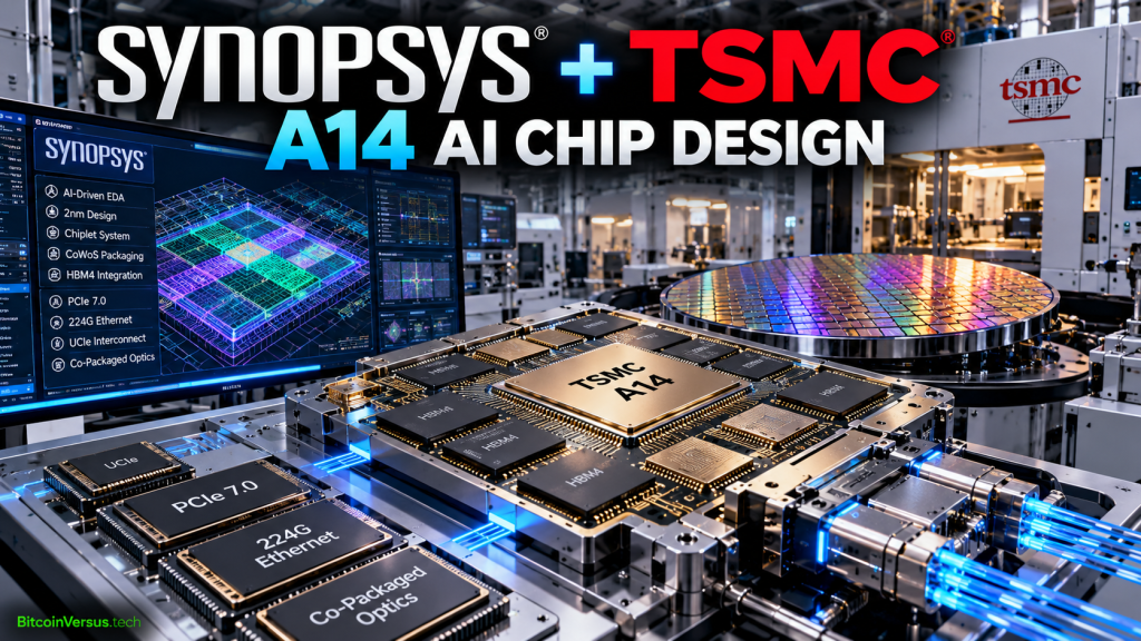
Synopsys and TSMC have expanded their collaboration around next-generation semiconductors, certifying design flows for TSMC’s A14 process while adding agentic AI workflows for complex chip development.
The September 23 announcement reaches well beyond one process node. The companies are also working across CoWoS advanced packaging, integrated voltage regulation, co-packaged optics, HBM4, PCIe 7.0, UCIe and 224G Ethernet PHY technology for future AI, HPC and data-center systems.
Agentic AI enters advanced chip design
Synopsys says its digital and analog EDA flows are certified for TSMC A14. The collaboration also applies agentic AI to analog, digital and multi-die workflows, including chiplet floorplan co-optimization through the Synopsys 3DIC Compiler platform.
HBM4, PCIe 7.0 and 224G Ethernet
On TSMC’s N2P process, Synopsys reports IP enablement and tape-out milestones covering PCIe 7.0, HBM4, LPDDR6/5X/5, 224G Ethernet PHY and UCIe. Those technologies address the information technology bottlenecks surrounding modern accelerators: memory bandwidth, die-to-die connectivity and high-speed networking.
The companies also demonstrated 32G/40G UCIe silicon on a TSMC N3P test chip integrated with a CoWoS-S interposer. Synopsys says it has completed 64G UCIe IP tape-outs on both 2 nm and 3 nm process nodes.
Power and optics become part of chip design
Integrated voltage regulators are being added to the CoWoS multi-die design workflow to address power integrity and efficiency. Synopsys and TSMC are also extending co-packaged-optics design through TSMC COUPE, combining photonic and electronic design with thermal and electrical analysis.
That matters because the limits of next-generation AI systems increasingly sit outside the compute core itself. Electricity, memory, packaging, fiber and Ethernet connectivity increasingly determine how much useful compute can be delivered.
The infrastructure stack keeps converging
BitcoinVersus.tech has been following the same convergence from the facility side through ABB’s 800 VDC AI data-center power system, Supermicro’s Vera Rubin rack systems, and Samsung’s AI-RAN networking and robotics work.
Sources: Synopsys and TSMC ecosystem materials.
Advertisement / Support BitcoinVersus.tech
Support independent technical reporting and research at BitcoinVersus.tech.
BitcoinVersus.Tech Editor’s Note & Disclaimer:
We volunteer daily to ensure the credibility of the information on this platform is Verifiably True. BitcoinVersus.tech provides news, technical analysis and educational information and does not provide financial or investment advice. Verify technical specifications and operational requirements with the manufacturer before making purchasing, deployment or investment decisions. If you would like to support to help further secure the integrity of our research initiatives, please donate here: 3C9o19EH5HSiwEPyCTmEKzxhNCbo2X6TTb


Leave a Reply