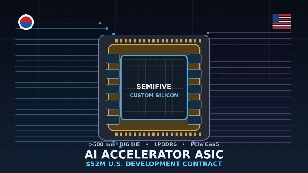
South Korean custom-silicon company SEMIFIVE has signed a contract worth approximately $52 million with an unnamed U.S. AI fabless company to develop a next-generation data-center inference accelerator, marking one of the company’s largest North American ASIC wins to date.
The announcement says the project will use SEMIFIVE’s end-to-end custom silicon model, covering architecture implementation, physical design, verification, packaging and manufacturing support. Independent distribution of the release places the deal at roughly KRW 70.3 billion.
The Chip Targets Data-Center AI Inference
The accelerator is being designed for inference workloads, including large language models, and is expected to use a die larger than 500 square millimeters. SEMIFIVE says the design will integrate LPDDR6 memory interfaces, PCIe Gen5 connectivity and its large-die implementation technology.
A die above 500 mm² pushes well beyond ordinary client silicon. Larger dies increase the challenge of power delivery, thermal control, signal integrity and manufacturing yield, which makes physical implementation and packaging as important as the accelerator architecture itself.
That design problem connects directly with other hardware trends BitcoinVersus.tech has been following, including SK hynix preparing HBM4 for mass production, onsemi embedding power devices into silicon for denser AI racks, Synopsys and TSMC applying agentic AI to advanced chip design, and Samsung bringing Mistral AI into semiconductor design and manufacturing.
LPDDR6 Shows a Different Memory Strategy
The use of LPDDR6 is notable because many high-end AI accelerators are associated with HBM. LPDDR can offer a different balance of bandwidth, cost, power and system complexity. For inference workloads that do not need the maximum bandwidth of HBM, that tradeoff can be attractive if the accelerator architecture is designed around it.
SEMIFIVE did not disclose the identity of the U.S. customer, the manufacturing process node, final transistor count, memory capacity or projected power envelope. Those omissions matter because they prevent a direct performance comparison with shipping accelerators from larger vendors.
Tape-Out Is Targeted for 2027
The development program is expected to move toward tape-out in 2027. Tape-out is the point at which the completed chip design is released for mask generation and fabrication, so the contract represents a development-stage program rather than a volume-shipping product today.
The contract also expands SEMIFIVE’s North American exposure after the company built much of its earlier custom-silicon business around Asian customers and Samsung Foundry manufacturing. A U.S. data-center accelerator win gives the company another route into the rapidly growing market for workload-specific AI chips.
Custom AI Silicon Keeps Expanding
The broader trend is that AI infrastructure buyers increasingly want chips tuned for specific workloads rather than relying exclusively on general-purpose GPUs. That is creating opportunity for design-service firms that can take a customer’s architecture and carry it through implementation, packaging and manufacturing.
SEMIFIVE has already moved a separate large-die AI inference accelerator into mass production using Samsung Foundry’s 4 nm process. The new $52 million U.S. contract is a different program, but it reinforces the same strategy: turning custom accelerator designs into manufacturable silicon without requiring the customer to build an entire chip-development organization internally.
The technical milestones to watch next are the selected process node, final memory configuration, package architecture and whether the unnamed customer reaches its 2027 tape-out target. Those details will determine how ambitious the accelerator really is and how quickly it can progress from contract to deployed data-center hardware.
BitcoinVersus.Tech Editor’s Note
Support independent technology reporting: BTC donations may be sent to 3C9o19EH5HSiwEPyCTmEKzxhNCbo2X6TTb.
Follow BitcoinVersus.tech on X/Twitter for AI hardware, semiconductors, Bitcoin mining and data-center reporting.
Disclaimer: BitcoinVersus.tech is not a financial advisor. This media platform reports on financial subjects purely for informational purposes.


Leave a Reply