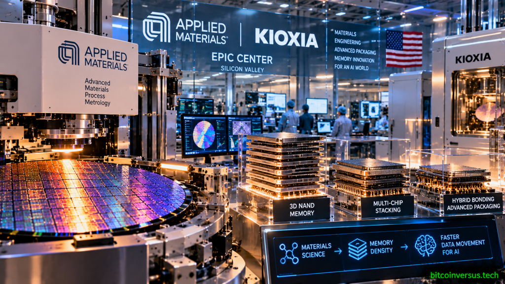
Applied Materials and KIOXIA are moving next-generation memory research into the same collaborative semiconductor lab, targeting the materials, stacking and packaging problems that increasingly determine how much useful AI compute a system can deliver.
The September 29 announcement says KIOXIA will join Applied Materials’ EPIC Center in Silicon Valley as an innovation partner. The companies plan joint work on advanced memory-cell and structure creation, multi-chip stacking, advanced packaging and materials engineering aimed at increasing memory density and performance for AI systems.
The collaboration places one of the world’s major flash-memory suppliers inside a $5 billion semiconductor-equipment R&D environment designed to shorten the distance between early process experiments and high-volume manufacturing. Applied says EPIC will be operationally ready this year, with capital spending scaling over time as customer projects begin.
AI memory is becoming a materials problem
AI accelerators do not benefit from more compute if data cannot move to and from memory fast enough. That pressure is pushing the industry toward denser structures, tighter integration, stacked dies and more sophisticated packaging rather than relying only on conventional planar scaling.
BitcoinVersus.Tech recently covered Micron’s 512GB DDR5 server module, showing how capacity is rising at the system-memory level. We also examined CoWoS-L packaging beyond reticle limits, where the same pressure to place more silicon closer together appears at the package level.
Early market coverage of the partnership likewise highlighted advanced memory cells, multi-chip stacking and new materials engineering as the core areas of work.
One real-time industry post summarized the project as a push to increase memory density and performance while Applied ramps EPIC Center investment.
The EPIC Center is built around co-development
Applied Materials is positioning EPIC as a place where equipment makers, chip manufacturers, designers and research teams can work on process technology before those changes reach production fabs. That matters because a new memory structure is rarely just a device-design problem. It may require new deposition, etch, metrology, bonding, packaging and inspection steps to become manufacturable.
The following English-language Six Five Media interview with Applied Materials explains why 3D scaling, advanced packaging and closer compute-to-memory integration are becoming central to AI semiconductor roadmaps. The video is broader than the KIOXIA partnership, but it directly explains the manufacturing logic behind the collaboration.
KIOXIA brings flash and storage expertise into the same loop
KIOXIA’s role is especially interesting because AI memory discussions often center on HBM, while KIOXIA’s core business is NAND flash and SSDs. AI infrastructure needs both high-speed working memory near accelerators and enormous storage capacity for model data, checkpoints, vector databases and retrieval workloads.
The KIOXIA keynote below focuses on that storage side of the stack. It helps explain why a flash-memory company would want earlier access to materials and process co-development rather than treating storage as a separate downstream component.
A second same-day post linked directly to the new Applied Materials and KIOXIA announcement as it circulated through semiconductor markets.
Stacking changes what has to be tested
As memory becomes more three-dimensional, manufacturing problems compound. More layers and more dies create additional opportunities for alignment errors, interconnect defects, thermal issues and yield loss. The manufacturing stack therefore needs more precise process control and more aggressive inspection.
BitcoinVersus.Tech’s recent look at Teradyne’s Magnum E2 memory-test platform covers the other end of that chain: once higher-speed memory is built, production test has to keep up with rapidly changing interfaces and performance targets.
The important shift is earlier collaboration
The KIOXIA partnership does not announce a finished memory product, a new NAND generation or a commercial stacked-memory device. It establishes a shared development environment intended to make those future technologies easier to commercialize.
That distinction matters. Semiconductor roadmaps increasingly depend on solving device architecture, materials, process equipment and packaging problems together. The EPIC model is an attempt to pull those decisions forward, so equipment and process choices can be evaluated alongside the memory architecture instead of after it.
For AI infrastructure, the result could be more than denser storage. Better materials and packaging can reduce the physical distance data travels, increase usable bandwidth, improve energy efficiency and make higher-density memory systems easier to manufacture at scale.
BitcoinVersus.Tech
Advertisement: Follow BitcoinVersus.Tech for independent coverage of semiconductors, AI hardware, data centers, Bitcoin mining, ASICs, energy and open technology.
BitcoinVersus.Tech Editor’s Note:
We volunteer daily to ensure the credibility of the information on this platform is Verifiably True. If you would like to support to help further secure the integrity of our research initiatives, please donate here: 3C9o19EH5HSiwEPyCTmEKzxhNCbo2X6TTb
BitcoinVersus.tech is not a financial advisor. This media platform reports on financial subjects purely for informational purposes.


Leave a Reply