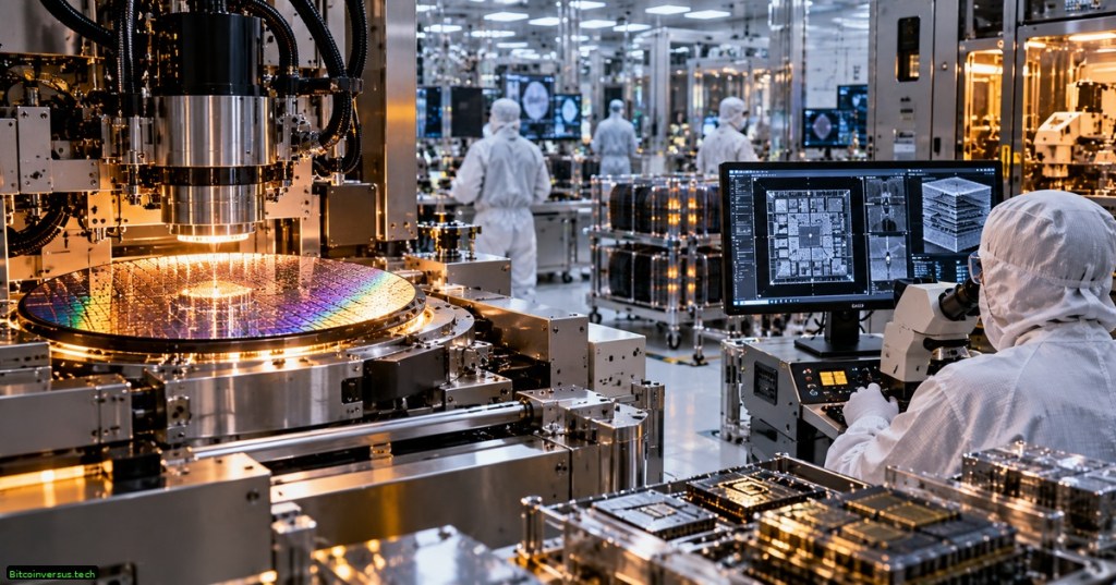
Applied Materials and Intel are tightening the loop between semiconductor equipment development and chip manufacturing by connecting Applied’s EPIC Center in Silicon Valley with Intel’s R&D campus in Hillsboro, Oregon. The October 6 collaboration targets the technologies underneath next-generation AI processors: transistors, interconnects, process integration and advanced packaging.
According to Applied Materials’ announcement, engineers from both companies will work across Applied’s EPIC Center and Intel’s Oregon technology-development organization to shorten the path from experimental materials and device structures to high-volume manufacturing.
The Collaboration Starts Below the Finished Chip
AI hardware performance is not determined only by how many transistors fit on a die. Modern processors also depend on how those transistors are built, how signals move through increasingly narrow interconnects, how power reaches each layer, how heat leaves the package, and how multiple dies communicate inside one system.
Applied and Intel say their joint work spans both front-end device development and back-end-of-line interconnect scaling. The front end is where transistor structures are formed in the silicon wafer. Back-end-of-line processing builds the metal wiring stack that connects those devices into working circuits.
As dimensions shrink, both parts of the process become harder to optimize independently. Changes in deposition, etch, dielectric materials, metals and interface control can determine whether a promising transistor or wiring concept can actually be manufactured at acceptable yield.
Foveros Makes Packaging Part of the Compute Architecture
A major part of the partnership is Foveros-based 3D stacking. Instead of treating packaging as the final box around a completed processor, Foveros lets Intel place active dies on top of other dies and connect them with extremely dense vertical links.
Intel’s technical documentation describes Foveros Direct 3D as direct copper bonding that can attach chiplets to active base tiles at very fine interconnect pitches. Higher connection density can reduce the distance data travels between logic, cache, memory interfaces and other specialized silicon.
This is closely related to the industry’s broader move toward hybrid bonding, where electrical connections and mechanical bonding are combined at extremely small pitches. The smaller those links become, the more a multi-die package begins to behave like one tightly integrated computing system.
Power Delivery and Heat Are Scaling Problems Too
Applied says the work is intended to improve interconnect density, power delivery and thermal performance. Those are no longer secondary packaging concerns. High-performance AI systems push enormous currents through dense packages while many compute dies operate simultaneously.
If power has to travel through long, resistive paths, voltage drop and heat increase. If heat cannot move efficiently out of vertically stacked silicon, sustained workload performance can suffer. Better packaging therefore becomes another path to higher system-level efficiency.
Intel has already been reorganizing server processors around increasingly modular chiplet architectures. The same manufacturing logic also supports the company’s Intel 18A roadmap, where transistor, power-delivery and packaging advances have to work together rather than arrive as isolated improvements.
EPIC Is Trying to Compress the R&D Timeline
The practical value of the EPIC model is proximity. Equipment engineers, materials scientists and chipmakers can test new process ideas using manufacturing-relevant hardware earlier instead of developing each piece in isolation and discovering integration problems years later.
Applied has already brought memory and packaging companies into the same model. Its work with KIOXIA uses the EPIC Center for next-generation memory R&D, while its expanded partnership with Besi pushes packaging development from wafer-level hybrid bonding toward broader die and panel architectures.
Intel adds something different: a leading-edge logic manufacturer with a large U.S. process-development organization. Connecting Hillsboro directly to Applied’s equipment-development environment could let transistor, wiring and package concepts be evaluated against real foundry requirements much earlier.
Why This Matters for AI Hardware
The AI-chip race is increasingly a race across the entire manufacturing stack. Architecture still matters, but future performance gains also depend on new transistor structures, shorter and lower-resistance interconnects, denser 3D integration, better thermal paths and manufacturing processes that can produce all of those features reliably.
That is also why semiconductor-equipment companies are becoming more visible in AI infrastructure. A new accelerator design cannot ship at scale unless wafer fabrication, packaging, inspection, metrology and process control all advance with it.
Applied and Intel are effectively trying to shorten that feedback loop. The objective is not merely a faster laboratory experiment. It is to move viable transistor, interconnect and 3D-packaging ideas from research into manufacturable AI hardware before the next architecture cycle passes them by.
BitcoinVersus.Tech
Advertisement
Editor’s Note
We volunteer daily to ensure the credibility of the information on this platform is Verifiably True. If you would like to support to help further secure the integrity of our research initiatives, please donate here: 3C9o19EH5HSiwEPyCTmEKzxhNCbo2X6TTb
BitcoinVersus.tech is not a financial advisor. This media platform reports on financial subjects purely for informational purposes.


Leave a comment