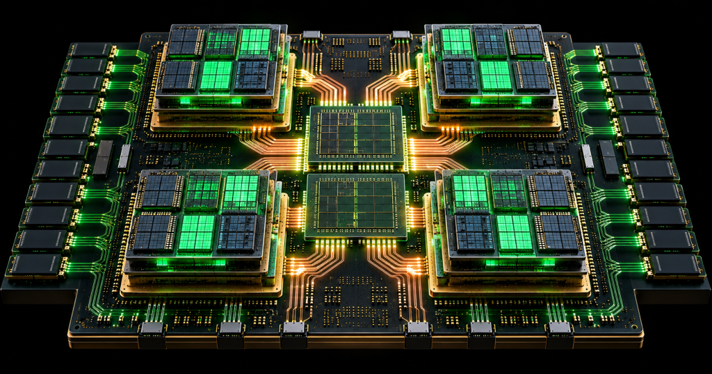
Intel’s next Xeon is not just a bigger server CPU. Diamond Rapids is a package-level redesign that turns the processor into a network of chiplets, cache tiles, and centralized fabric hubs connected through UCIe.
Intel used Hot Chips 2026 to detail the architecture of its next-generation Xeon 7 platform. The company’s official Hot Chips presentation describes Diamond Rapids as its next major Xeon design for 2027, built around a highly disaggregated package rather than one large monolithic compute die.
Tom’s Hardware summarized the architecture in an August 24 X post: up to 256 P-cores, as much as 1.28 GB of last-level cache, AVX 10.2, and UCIe-S replacing EMIB for critical package-level communication.
Sixteen Core Chiplets Feed Four Compute Building Blocks
Diamond Rapids divides its compute resources into what Intel calls Compute Building Blocks, or CBBs. Each CBB can hold four core chiplets, and each chiplet can contain up to 16 P-cores.
Scale that across four CBBs and the full package reaches 16 core chiplets and up to 256 cores. The core chiplets are built on Intel’s 18A-P process, while the base tiles beneath them use Intel 3-T.
That makes Diamond Rapids another example of the server CPU becoming a collection of specialized dies rather than a single piece of silicon. BitcoinVersus.Tech just covered Fujitsu MONAKA moving its last-level cache onto separate 5 nm SRAM dies, and Intel is making a related decision here: put different functions on different pieces of silicon, then connect them tightly enough that software still sees one processor.
The Base Tile Holds the Shared Cache
Inside each CBB, the core chiplets sit above a base tile connected with Intel’s Foveros Direct 3D technology. The core chiplets contain private L2 cache, while the shared L3 cache is located on the base tile underneath.
This arrangement separates hot, high-performance core logic from the larger shared-cache structures while keeping the two physically close. That is increasingly important because SRAM scaling has become one of the hardest parts of advanced CPU design.
Across the full processor, Intel is targeting up to 1.28 GB of last-level cache. At that scale, cache placement is no longer a minor floorplanning choice. It affects die area, power, latency, thermal density, and how efficiently hundreds of cores can share data.
Intel Put the Memory and I/O in the Middle
Diamond Rapids also reverses the spatial logic of some earlier Xeon designs. The four compute blocks sit around the outside of the package, while two centralized Fabric Hub Tiles sit in the middle.
Those fabric hubs aggregate the memory and I/O subsystems. Intel says the design supports 16 DDR5 memory channels, up to 8,000 MT/s with conventional DDR5 and up to 12,800 MT/s with MRDIMMs.
The I/O subsystem also scales to 128 lanes that can be used for PCIe 6.0, CXL 3.0, UPI, or combinations of those interfaces. That is a major amount of external connectivity for one socket and reflects how much more work the CPU has to coordinate in an AI-era server.
The same pressure is visible in BitcoinVersus.Tech’s recent coverage of IBM’s dual-ISA Arm and z/Architecture processor. Modern server CPUs are being redesigned around data movement and system integration as much as around raw integer execution.
Why Intel Chose UCIe-S Instead of EMIB
One of the more interesting packaging decisions is what Intel did not use. Diamond Rapids does not rely on Intel’s familiar EMIB bridge to connect the compute regions to the central fabric hubs.
Instead, Intel uses UCIe-S through copper wiring in the package substrate. Independent Hot Chips coverage reports that Intel chose UCIe-S because it provided a more uniform low-latency connection across the package distance between each CBB and both fabric hubs.
That distinction matters. Advanced package links are not automatically better just because they are denser or more exotic. The physical distance, signaling requirements, latency target, power budget, routing flexibility, and manufacturing cost all shape which interconnect makes sense.
Diamond Rapids therefore turns UCIe into something more than a generic chiplet standard. It becomes part of the CPU’s internal topology.
The Package Starts to Look Like a Tiny Network
With 16 core chiplets, four base tiles, and two fabric hubs, Diamond Rapids is easier to understand if the package is treated like a small network.
Each compute block has to reach both central hubs. The hubs maintain access to memory and external I/O. Cache coherency has to work across the whole socket. Traffic needs to avoid pathological bottlenecks as hundreds of cores generate memory, I/O, and coherence requests at the same time.
That makes routing and topology first-class CPU-design problems. Once the package becomes this disaggregated, performance depends on how well the fabric moves data between dies, not just how fast the individual cores execute instructions.
Moving the Hot Cores Outward May Help Cooling
The physical layout has a thermal benefit too. By pushing the core-heavy compute blocks toward the perimeter and putting the more centralized memory and I/O fabric in the middle, Intel reduces the concentration of the hottest logic at the center of the package.
That can make cold-plate design and heat spreading easier, especially in high-power server configurations. At this scale, package topology is thermal architecture.
Fujitsu’s MONAKA story makes the same broader point from another direction: once CPUs are assembled from multiple dies and layers, thermal paths become part of the architecture itself.
Diamond Rapids Also Modernizes the x86 ISA
The package gets most of the attention, but Diamond Rapids also brings major instruction-set changes.
Intel is moving Xeon to AVX 10.2 and Advanced Performance Extensions, or APX. APX expands the number of general-purpose registers from 16 to 32, giving compilers more room to keep values close to the execution units and reduce unnecessary loads and stores.
That makes Diamond Rapids interesting from both sides of processor design. The physical package is becoming more distributed, while the software-visible x86 architecture is gaining more registers and newer vector capabilities.
That contrast also connects with BitcoinVersus.Tech’s recent look at NUVACORE’s Core First architecture. NUVACORE is trying to postpone the ISA choice. Intel is doing the opposite: preserving x86 compatibility while rebuilding nearly everything around how the cores communicate inside the package.
The Server CPU Is Becoming a System in a Package
Diamond Rapids shows how far server CPUs have moved beyond the old image of one die surrounded by memory controllers.
The processor now contains leading-edge core chiplets, separate base tiles, giant shared caches, centralized fabric hubs, 3D die stacking, substrate-level UCIe links, 16 memory channels, and 128 lanes of external high-speed I/O.
That is closer to a miniature data center fabric than a traditional single-die CPU.
The core architecture still matters, but Diamond Rapids makes another point just as clearly: in a modern Xeon, the package is becoming part of the microarchitecture.
BitcoinVersus.Tech
Advertisement
Editor’s Note:
We volunteer daily to ensure the credibility of the information on this platform is Verifiably True. If you would like to support our research initiatives, please donate here: 3C9o19EH5HSiwEPyCTmEKzxhNCbo2X6TTb
BitcoinVersus.tech is not a financial advisor. This media platform reports on financial subjects purely for informational purposes.


Leave a Reply