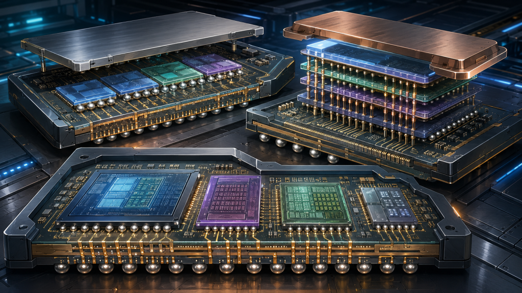
Two-dimensional semiconductor packaging places a single die or multiple dies on the same horizontal plane inside a package.
Signals travel through wire bonds, solder bumps, redistribution layers, or package-substrate traces before reaching the printed circuit board.
This mature approach remains widely used because it is generally less expensive, easier to manufacture, and simpler to inspect, test, and cool.
Three-dimensional semiconductor packaging stacks active dies vertically and connects them through technologies such as microbumps, hybrid bonding, or through-silicon vias.
These shorter vertical connections can increase bandwidth, reduce signal distance, improve interconnect density, and reduce the package footprint.
Three-dimensional packaging is especially valuable for artificial intelligence processors, high-performance computing, advanced memory, and compact electronic systems.
The main difference is physical arrangement rather than chip function. Two-dimensional packaging prioritizes manufacturing simplicity and cost, while three-dimensional packaging prioritizes density, bandwidth, and system-level performance.
Both approaches will remain important because many products do not require the added cost, thermal management, and manufacturing complexity associated with vertically stacked semiconductor dies.
BitcoinVersus.Tech Editor’s Note:
We volunteer daily to ensure the credibility of the information on this platform is Verifiably True. If you would like to support to help further secure the integrity of our research initiatives, please donate here: 3C9o19EH5HSiwEPyCTmEKzxhNCbo2X6TTb
BitcoinVersus.tech is not a financial advisor. This media platform reports on financial subjects purely for informational purposes.


Leave a Reply