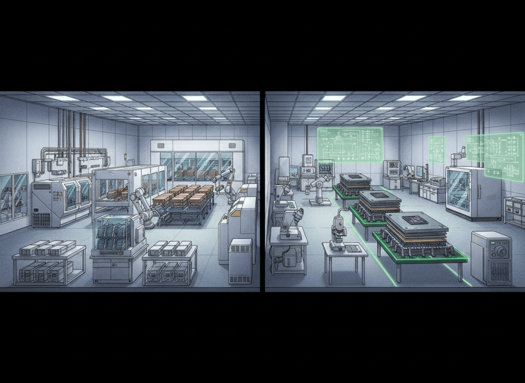
Taiwan has broken ground on the Baipu Industrial Park in Kaohsiung, where TSMC plans to establish an advanced semiconductor packaging validation laboratory and talent-training center.
The project is aimed at a growing bottleneck in AI hardware: validating the equipment and materials required for increasingly complex advanced packaging. TSMC’s packaging technologies are used in AI chips designed by companies including Nvidia, AMD and Broadcom.
The Baipu park covers about 88.7 hectares, with roughly 53.6 hectares designated for industrial use. TSMC is expected to build two facilities: a technology-validation laboratory and a semiconductor talent-training center. Operations are targeted for the fourth quarter of 2029.
TSMC previously said its planned three-hectare site would use modular cleanrooms and laboratories for joint testing of advanced packaging technologies, equipment and materials. The company estimates the setup could improve validation efficiency by 25% to 50%.
Advanced packaging has become central to AI accelerator design because modern systems increasingly combine multiple compute dies, high-bandwidth memory and dense interconnects in one package. BitcoinVersus.tech’s 2D vs. 3D semiconductor packaging guide explains how these packaging approaches differ, while our coverage of new AI chip packaging equipment tracks the manufacturing hardware supporting the transition.
According to Reuters, the park is intended to let equipment and materials suppliers perform research, testing and validation closer to TSMC, potentially shortening the path from development to mass production.
BitcoinVersus.Tech Editor’s Note:
We volunteer daily to ensure the credibility of the information on this platform is Verifiably True. If you would like to support to help further secure the integrity of our research initiatives, please donate here: 3C9o19EH5HSiwEPyCTmEKzxhNCbo2X6TTb
BitcoinVersus.tech is not a financial advisor. Information is provided for informational purposes.


Leave a Reply