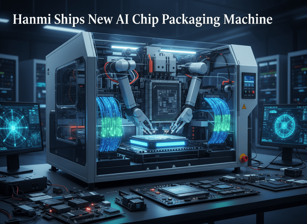
Hanmi Semiconductor has shipped its first FC Bonder 75, pushing deeper into the advanced-packaging equipment needed to build increasingly large AI processors.
The South Korean equipment maker said the system supports 2.5D AI semiconductor packaging using interposers as large as 75 mm × 75 mm. That is a major step up from conventional package dimensions and gives manufacturers room to integrate large logic dies with high-bandwidth memory and other chiplets.
Why the package is getting bigger
Modern AI accelerators are no longer defined by one monolithic die. CPUs, GPUs, HBM stacks and specialized I/O increasingly have to operate as one tightly connected system. The package itself is therefore becoming part of the performance architecture.
That shift is driving investment in 2.5D packaging. A large interposer provides dense, short electrical paths between separate dies, helping move enormous amounts of data without forcing every function onto the same piece of silicon. Recent TrendForce research on advanced AI packaging likewise highlights the industry’s move toward packages that extend beyond traditional reticle-size constraints.
The manufacturing equipment matters
The FC Bonder 75 is interesting because the AI race is increasingly an equipment story as much as a GPU story. Building larger heterogeneous packages requires precise placement, bonding, thermal control, inspection and yield management. A theoretically powerful chip architecture has little commercial value if manufacturers cannot assemble it repeatedly at acceptable yield.
Hanmi has been expanding beyond its established HBM-related TC bonders with additional 2.5D systems. The company says its 2026 lineup includes the FC Bonder 3.5 and multiple 2.5D TC Bonder platforms, with another larger system planned.
A useful advanced-packaging primer
The video above from Applied Materials provides a useful visual explanation of advanced packaging, including logic chiplets and stacked memory. Those are the same broad integration pressures making equipment such as large-format bonders increasingly important.
What to watch next
The next question is not simply who can design the fastest AI accelerator. Watch the companies that can manufacture the interposers, bonding systems, substrates, HBM stacks, cooling systems and inspection equipment needed to turn those designs into high-volume hardware.
Hanmi also plans to establish Hanmi USA in October, positioning the equipment maker closer to U.S. AI, foundry, OSAT and memory customers. As AI packages become physically larger and electrically denser, advanced packaging capacity may become one of the less visible constraints determining how quickly new compute platforms can scale.
BitcoinVersus.Tech Editor’s Note:
We volunteer daily to ensure the credibility of the information on this platform is Verifiably True. If you would like to support to help further secure the integrity of our research initiatives, please donate here: 3C9o19EH5HSiwEPyCTmEKzxhNCbo2X6TTb


Leave a Reply