Elementary Overview
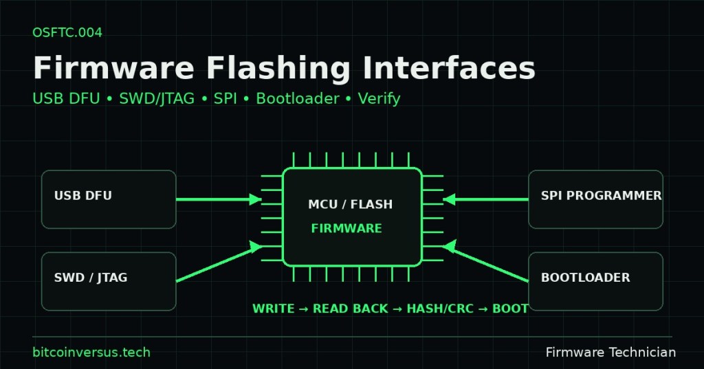
Firmware flashing means writing a new program image into nonvolatile memory so a device can boot and run it later. The same firmware file can sometimes be written through several different paths: a built-in USB bootloader, a SWD/JTAG debug probe, a serial bootloader, or a direct SPI flash programmer. The technician’s first job is therefore not simply to “flash the file,” but to identify the correct hardware, memory device, interface, voltage, image, and recovery path. This lesson builds on OSFTC.002 serial consoles and OSFTC.003 backup and recovery.
Choose the Flashing Path Before Connecting a Programmer
The correct flashing path depends on the device architecture and the failure state. A working device may accept a signed update through its normal application, while a partially broken device may need a ROM bootloader, SWD/JTAG probe, or direct flash access. Check the board schematic, service manual, microcontroller memory map, flash part number, and boot-mode straps before attaching anything. Confirm logic voltage as well: 1.8 V, 3.3 V, and 5 V interfaces are not automatically interchangeable. On boards such as ESP32- or STM32-based systems, boot pins and reset sequencing decide whether the processor starts the normal application or enters a programming mode. Technician work should begin with identification, not trial-and-error wiring.
USB DFU Uses a Bootloader Instead of an External Debug Probe
USB Device Firmware Upgrade (DFU) lets supported hardware receive firmware over USB while a bootloader controls the erase and write operations. This can be convenient because no external debug probe is required, but the device must enter the correct DFU state and the image must target the correct memory layout. A typical workflow is: identify the DFU device, verify the firmware file, program it, reset the device, then confirm the new version and normal boot. Do not assume a file with a familiar name is correct; compare version, hardware revision, expected size, and checksum against the approved release. The same principle applies to practical update workflows such as Bitaxe firmware updating.
SWD and JTAG Provide Low-Level Access to Internal Flash
SWD and JTAG let a debug probe communicate directly with a microcontroller’s debug interface. For technician flashing, that means the probe can often identify the target, halt the CPU, erase or program internal flash, verify the result, and reset the device even when the normal application will not boot. Common probes include ST-Link and SEGGER J-Link. Match the target voltage reference, ground, clock/data pins, reset wiring, and processor family before programming. A useful OpenOCD-style workflow is program firmware.elf verify reset exit, because writing without read-back verification leaves a major uncertainty unresolved.
Direct SPI Programming Is the Recovery Path When the Host Cannot Help
Some systems store firmware in an external SPI NOR flash chip. If the processor, bootloader, or motherboard firmware is too damaged to perform an in-system update, a technician may read and write that flash directly with a programmer such as a CH341A-class device or a professional in-circuit programmer. Before writing, read the original chip more than once, compare the dumps, save the known-good backup, confirm the flash-part ID, and make sure the programmer voltage matches the chip. In-circuit programming can be complicated by other components loading the SPI bus, so a clip that physically fits is not proof that the electrical setup is safe. This is exactly why the backup discipline from OSFTC.003 comes before erase/write operations.
Serial Bootloaders Turn UART or USB Into a Recovery Channel
Many microcontrollers contain a factory ROM bootloader or a project-specific bootloader that accepts firmware through UART, USB, CAN, Ethernet, or another interface. On ESP32 systems, for example, esptool communicates with the chip’s serial bootloader and writes specific images to specific flash offsets. The important technician concept is that a firmware image is not always one monolithic file: bootloader, partition table, application, calibration, or configuration regions may occupy different addresses. Writing the right bytes to the wrong offset can still produce a non-booting device. Capture the serial boot log after flashing so you can tell whether the bootloader, application, or hardware initialization failed.
A Successful Write Is Not a Successful Repair Until It Is Verified
Always separate write completion from functional validation. The programmer should first verify memory contents by read-back comparison, CRC, hash, or the tool’s own verify operation. Then reset the device and inspect the first boot for version, hardware detection, configuration migration, watchdog resets, unexpected recovery loops, and peripheral initialization. If the image uses secure boot or signed firmware, signature validation may reject a file that was electrically written without error. Save the programmer log and post-flash boot log as evidence. A robust update path therefore looks like: backup → identify → erase/write → verify → reset → boot-log check → functional test → rollback readiness.
Useful Command Examples
# List USB DFU devices
dfu-util -l

# Identify an ESP32-family target before any change
esptool --port /dev/ttyUSB0 chip-id

# Confirm the installed OpenOCD tool version
openocd --version

# Verify the approved firmware file checksum
sha256sum firmware.bin
Technician Flashing Checklist
- Identify device model, board revision, microcontroller, and flash part.
- Confirm the approved firmware version and file checksum.
- Back up existing flash or configuration when possible.
- Choose the correct interface: application updater, DFU, UART bootloader, SWD/JTAG, or direct SPI.
- Confirm logic voltage, ground, pinout, reset, and boot-mode straps.
- Record current firmware version and serial/asset information.
- Perform erase/write using the manufacturer-approved tool or documented open-source equivalent.
- Run the tool’s verify/read-back operation.
- Reset or power-cycle according to the procedure.
- Capture the first boot log and confirm the expected firmware version.
- Test critical peripherals and configuration.
- Keep the backup, logs, checksum, tool version, and rollback method with the work record.
Exercises
- Given a board with USB DFU and SWD access, explain when you would choose one over the other.
- Describe the risks of connecting a 3.3 V SPI flash to a programmer configured for the wrong voltage.
- Write a recovery sequence for a device whose application is corrupt but whose ROM bootloader still responds.
- Explain why two matching backup reads are stronger evidence than one successful read.
- List the evidence you would save after flashing ten identical devices in a production-support job.
- Explain the difference between memory verification and functional validation.
Knowledge Check + Answers
- What is DFU? A bootloader-based method for downloading firmware to supported hardware over USB.
- Why use SWD/JTAG? It provides low-level access for programming, target identification, debugging, and recovery when the normal application path is unavailable.
- Why back up SPI flash before writing? The original chip may contain unique calibration, serial, configuration, or recoverable firmware data.
- What is a flash offset? The address where a particular image or region is stored within flash memory.
- What does verify mean? Confirming that the bytes actually stored in flash match the intended image, usually by read-back comparison, hash, CRC, or programmer verification.
- Why inspect the first boot log? A verified write can still fail during boot because of configuration, compatibility, signature, hardware, or initialization problems.
Elementary Conclusion
A firmware technician can think of flashing as choosing the safest door into a device’s memory. USB DFU is one door, SWD/JTAG is another, a serial bootloader is another, and a direct SPI programmer is the emergency door when the processor cannot help. The important part is not how quickly the new file can be written. The important part is knowing that the file belongs to the hardware, the voltage and wiring are correct, the old data is recoverable, the new bytes were written correctly, and the device actually boots and works afterward. A careful technician always leaves evidence and a recovery path instead of treating “program completed” as the end of the job.
BitcoinVersus.Tech
Advertisement
Editor’s Note:
We volunteer daily to ensure the credibility of the information on this platform is Verifiably True. If you would like to support our research initiatives, please donate here: 3C9o19EH5HSiwEPyCTmEKzxhNCbo2X6TTb
BitcoinVersus.tech is not a financial advisor. This media platform reports on financial subjects purely for informational purposes.


Leave a comment