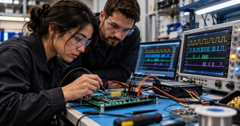
Elementary Overview
SPI troubleshooting is the process of proving whether a host and peripheral are exchanging the right bits at the right time on the right wires. A device can have correct firmware and correct power yet still fail because the clock mode is wrong, chip select never asserts, MOSI/MISO are reversed, logic levels are incompatible, timing is marginal, or two devices drive the bus at once.
This lesson follows OSFTC.007: SPI NOR Flash Diagnostics. That lesson focused on the memory device. OSFTC.008 widens the scope to the bus itself so the same method applies to flash chips, ADCs, DACs, displays, sensors, radios, controllers, and other SPI peripherals.
It also builds on OSFTC.006: I²C Bus Troubleshooting. Both are synchronous serial buses, but SPI normally uses separate clock, transmit, receive, and chip-select signals rather than open-drain SDA/SCL wiring and addressing on a shared two-wire bus.
Know The Four Core Signals
Microchip’s current SPI overview describes the common four-signal arrangement: serial clock, host-to-client data, client-to-host data, and chip select. Names vary by vendor, but the functions remain recognizable.
- SCLK / SCK: serial clock generated by the host.
- MOSI / SDO: data traveling from host to peripheral.
- MISO / SDI: data traveling from peripheral to host.
- CS / SS / NSS: chip-select signal that activates the intended peripheral, commonly active low.
Always confirm signal naming from the actual schematic and datasheet. One vendor may label pins from the controller’s perspective while another labels them from the device’s own input/output perspective.
SPI Is Full Duplex, But Many Transactions Are Functionally One-Way
SPI shifts one bit out while shifting one bit in on each clock cycle. That makes the electrical interface full duplex. But a command may still be functionally one-way. A flash device might receive an opcode and address on MOSI before returning useful data on MISO. During other clocks, one side may shift dummy bits simply because clocks are required to move the response.
Do not assume that “00” or “FF” on one data line means failure until you understand the transaction format. Read the peripheral datasheet and compare the expected opcode, address width, dummy cycles, and response sequence with the actual capture.
Start With Power, Ground, And Logic Levels
Before decoding bytes, verify the electrical basics. Confirm peripheral supply voltage, ground continuity, reset state, enable pins, and the logic voltage used by the host and peripheral. A 1.8 V peripheral connected directly to a 3.3 V host may require level translation depending on the device ratings.
Use a multimeter for static rails and an oscilloscope for signal levels and edge quality. A logic analyzer tells you whether the digital pattern makes sense; an oscilloscope tells you whether the waveform itself is electrically healthy.
This evidence-first approach matches the safe flashing workflow from OSFTC.004: Firmware Flashing Interfaces: identify the interface and voltage before connecting a programmer or probe.
Chip Select Defines The Transaction Boundary
In a common SPI transaction, the host asserts chip select, generates clock pulses while exchanging data, then releases chip select. The peripheral may use that transition to reset an internal bit counter, latch a command, or complete a write or read operation.
If chip select never goes active, the peripheral may ignore the clock and MOSI traffic. If it toggles too early, the command can be cut short. If it stays active across transactions that the device expects to be separate, bytes may be interpreted in the wrong state.
With multiple peripherals sharing SCLK, MOSI, and MISO, each device normally has its own chip-select line. Microchip’s SPI application note describes the host selecting one client by asserting its SS line while the shared data and clock wiring serves the bus.
CPOL And CPHA Create Four SPI Modes
Two settings determine the relationship between clock and data: clock polarity and clock phase. CPOL defines the idle state of the clock. CPHA defines which clock edge is used for sampling relative to when data changes.
The combinations are commonly called SPI modes 0, 1, 2, and 3. A host configured for the wrong mode can show perfectly regular clock pulses while decoding every byte incorrectly.
- Mode 0: CPOL 0, CPHA 0.
- Mode 1: CPOL 0, CPHA 1.
- Mode 2: CPOL 1, CPHA 0.
- Mode 3: CPOL 1, CPHA 1.
The peripheral datasheet is authoritative. Do not pick a mode because another device on the board uses it.
Saleae Support — official Logic 2 protocol-analyzer walkthrough using SPI captures and showing how sampling-edge settings affect decoding.
A Logic Analyzer Shows Protocol Timing Clearly
Saleae’s SPI analyzer guide supports assigning clock, MOSI, MISO, and enable/chip-select channels and configuring the sampling edge, bit order, and other decode settings. This makes the tool useful for comparing the electrical transaction with the peripheral datasheet.
Capture enough channels to prove the transaction, not merely the data line. At minimum, capture SCLK, CS, and whichever data line matters. For full duplex troubleshooting, capture both MOSI and MISO.
Set the digital threshold appropriately for the logic voltage. Sample much faster than the SPI clock so timing edges are represented accurately. If the analyzer sample rate is too low, the decode can be wrong even though the target hardware is working correctly.
The Oscilloscope Finds Problems A Decoder Can Hide
A protocol decoder may label bytes correctly while the underlying signal is marginal. Use an oscilloscope when you suspect ringing, overshoot, undershoot, slow edges, crosstalk, incorrect thresholds, or timing margin problems.
Rohde & Schwarz’s SPI debugging material shows the relationship between raw analog signals, digital thresholds, protocol assignment, and decoded frames. The analog waveform matters because the receiver sees voltage and timing—not the convenient hex values displayed by the decoder.
Rohde & Schwarz — official SPI decode tutorial covering channel assignment, mode, thresholds, triggering, and decoded results.
Check Clock Frequency Against The Peripheral Limit
The host controls SCLK frequency. A peripheral that supports 20 MHz SPI under one supply and temperature condition may support less under another. Read the timing characteristics rather than relying on a generic “SPI is fast” assumption.
A practical diagnostic is to lower the SPI clock substantially. If the system suddenly becomes reliable, investigate timing margin, signal integrity, level translation, loading, firmware delays, and board layout rather than declaring the peripheral defective.
SparkFun’s SPI reference also emphasizes SPI as a short-distance interface and notes that reducing clock speed can help when signal integrity becomes problematic over longer interconnects.
Bit Order And Word Length Can Make Good Waveforms Look Like Bad Data
Many devices send the most-significant bit first, but some use least-significant-bit-first operation or word sizes other than eight bits. A decoder configured for eight-bit MSB-first traffic can produce nonsense from a valid 16-bit or LSB-first transfer.
Compare the waveform against the peripheral command format. Check whether commands are 8, 16, 24, or 32 bits, whether addresses are included, and whether data fields cross byte boundaries.
MISO Must Release The Bus When The Device Is Not Selected
When multiple peripherals share MISO, normally only the selected peripheral may drive the line. Other devices should present a high-impedance output. If two peripherals drive opposite logic states simultaneously, the bus is contending.
Symptoms can include incorrect returned bytes, abnormal intermediate voltage, excess current, or failures that occur only when a second device is populated or enabled. Use chip-select traces and the oscilloscope to determine whether more than one device is driving MISO.
This is one reason Microchip’s SPI documentation states that only one client should transmit back to the host during a given transfer.
SPI Flash Adds Command-Specific Clues
For SPI NOR flash, connect the bus-level observations back to OSFTC.007. Useful transactions include JEDEC identification reads, status-register reads, address cycles, read commands, write-enable commands, program/erase operations, and busy polling.
If the host sends a valid Read JEDEC ID opcode but MISO never responds, inspect power, chip select, reset/hold pins, logic voltage, MISO continuity, and whether the device is actually the part you think it is. If the response is present but decoded incorrectly, inspect SPI mode, bit order, analyzer threshold, and sampling edge.
A current Saleae community example shows the same debugging philosophy in practice: capture the real electrical behavior on the bench and use mixed-signal evidence to isolate firmware and hardware faults instead of assuming the code path is correct.
Saleae community example — mixed-signal bench debugging with a modern logic-analyzer/MSO workflow.
Use A Known-Good Transaction As A Reference
One of the most powerful troubleshooting techniques is comparing a failing board with a known-good board of the same revision and firmware. Capture the same boot phase or command on both systems, then compare chip-select timing, clock mode, frequency, MOSI command sequence, MISO response, delays, and voltage levels.
This reduces guesswork. If MOSI is identical but MISO differs, the problem is likely downstream of the host command. If both MOSI and clock differ, look earlier at firmware configuration, device-tree or board settings, boot stage, pin muxing, or hardware revision.
The hardware-revision discipline from OSFTC.006: Hardware/Firmware Compatibility matters here: two boards that look identical can route the same logical SPI peripheral through different pins or voltage domains.
Trigger On The Event You Care About
Long captures can contain thousands of valid transactions. Use chip-select transitions, a specific MOSI opcode, or a protocol-aware trigger to isolate the failure. A boot flash read, sensor-register access, or device-ID command is easier to interpret when the capture starts at the actual transaction of interest.
Saleae’s analyzer documentation and Digilent’s SPI debugging walkthrough both show how protocol-aware tools can turn clock/data waveforms into byte-level evidence while still letting the technician inspect the underlying signals.
OpenSecurityTraining2 — practical SPI-analysis hardware setup with a Saleae analyzer, useful for understanding probing and capture of real firmware traffic.
External Programmers Can Change The Bus
Connecting a programmer or analyzer is not always electrically invisible. A clip, long jumper wires, level shifter, powered programmer, or second controller can load the bus or back-power the target. This is especially important when working with onboard SPI flash.
Follow the isolation and backup practices from OSFTC.003: Firmware Backup and Recovery and OSFTC.004. Decide whether the target should be powered, unpowered, isolated, or held in reset based on the board design and programmer instructions.
Watch For Reset And Watchdog Effects
If the system repeatedly resets, the SPI capture may stop in the same place every boot. Correlate the bus with OSFTC.005: Watchdog Timers and Reset Loops and the serial logs from OSFTC.002: Serial Console and Boot Logs.
Example: if boot logs stop at “reading configuration” and the SPI trace shows a repeated ID command with no MISO response, the bus evidence and firmware log point to the same subsystem. If the SPI exchange completes normally but the watchdog resets later, the root cause likely lies elsewhere.
Technician Troubleshooting Order
- Identify the host, peripheral, board revision, expected logic voltage, and exact SPI pins.
- Confirm power, ground, reset, enable, hold, and write-protect states where applicable.
- Verify chip select reaches the intended peripheral.
- Measure SCLK frequency and idle polarity.
- Capture SCLK, CS, MOSI, and MISO with an appropriate logic analyzer sample rate.
- Configure the analyzer for the datasheet’s CPOL, CPHA, bit order, and word length.
- Compare MOSI commands with the peripheral protocol.
- Compare MISO responses with the expected reply.
- If decode is inconsistent, inspect raw analog waveforms with an oscilloscope.
- Reduce clock rate to test timing and signal-integrity margin.
- Check for MISO contention when multiple peripherals share the bus.
- Compare a failing board against a known-good capture when possible.
- Correlate bus behavior with serial boot logs, reset cause, and firmware stage.
- Remove probes or programmers and verify the device again in its normal configuration.
- Document the final waveform, decode settings, fault cause, and corrective action.
Technician Pattern Recognition
- No SCLK: inspect host initialization, pin mux, peripheral enable, reset state, and firmware execution point.
- SCLK and MOSI exist but CS never asserts: inspect GPIO assignment, polarity, pin mux, board revision, and driver configuration.
- MOSI looks correct but MISO stays flat: inspect peripheral power, CS, reset/hold pins, MISO continuity, bus contention, and device identity.
- Decoded bytes are nonsense but waveforms look clean: verify CPOL/CPHA, bit order, word length, thresholds, and channel mapping.
- Works at 1 MHz but fails at 20 MHz: investigate timing margin, loading, trace integrity, level translation, and peripheral frequency limits.
- MISO voltage sits between valid logic levels: investigate two devices driving the bus or a damaged output.
- Works with analyzer disconnected but fails while probing: inspect probe capacitance, ground lead length, clip loading, and test setup.
- Same command repeats until watchdog reset: correlate failed peripheral response with boot logs and reset-cause evidence.
Exercises
- A peripheral datasheet specifies SPI mode 3. Explain what you would verify in the captured clock before trusting the decoded bytes.
- A board has SCLK and MOSI activity but MISO remains high. Build a troubleshooting sequence that separates host, wiring, chip-select, and peripheral faults.
- Explain why lowering SPI frequency is a useful diagnostic even if production must eventually operate at the original speed.
- A shared MISO line measures about half the expected logic-high voltage during certain transactions. Explain what fault you would suspect and how you would prove it.
- Describe the difference between a logic analyzer and oscilloscope when troubleshooting SPI.
- Create a capture plan for comparing one known-good board with one failing board during boot-flash access.
- Explain why attaching an external SPI programmer can change the electrical behavior of the original bus.
Knowledge Check + Answers
- Who normally generates SCLK? The SPI host/controller.
- What does chip select do? It identifies which peripheral should participate in the transaction and often defines transaction boundaries.
- What do CPOL and CPHA control? Clock idle polarity and the relationship between clock edges and data sampling.
- Why capture both MOSI and MISO? To prove what the host commanded and what the peripheral returned.
- What does a logic analyzer do best? Capture and decode digital timing and protocol sequences across multiple channels.
- What does an oscilloscope add? Analog evidence such as voltage level, rise/fall time, ringing, overshoot, and noise.
- Why can multiple MISO drivers be dangerous? Two devices driving opposite states create bus contention and invalid voltage levels, and can stress outputs.
- Why can correct hex decode still be insufficient proof? The signal can be marginal electrically even when the current capture decodes correctly.
Prior Lessons And Primary References
- OSFTC.007 — SPI NOR Flash Diagnostics
- OSFTC.006 — I²C Bus Troubleshooting
- OSFTC.006 — Hardware/Firmware Compatibility
- OSFTC.005 — Watchdog Timers and Reset Loops
- OSFTC.004 — Firmware Flashing Interfaces
- OSFTC.003 — Firmware Backup and Recovery
- OSFTC.002 — Serial Console and Boot Logs
- OSFTC.001 — Firmware Images, Safe Flashing, Bootloaders, and Recovery Basics
- Microchip — Serial Peripheral Interface Peripheral
- Microchip Developer Help — SPI Introduction
- Saleae — SPI Analyzer User Guide
- Saleae — STM32 SPI Analysis Example
- Digilent — What Is SPI?
- Digilent WaveForms — Logic Analyzer SPI Interpreter
- Rohde & Schwarz — SPI Bus Decoding
Elementary Conclusion
SPI troubleshooting is a timing-and-evidence problem. First prove power, ground, reset, and logic voltage. Then prove chip select, clock, mode, MOSI command, and MISO response. Use the logic analyzer to understand transaction structure and the oscilloscope to verify electrical quality. Compare the capture with the peripheral datasheet and, when possible, with a known-good board. The best technician does not stop when the decoder shows hex bytes; the technician proves that the physical waveform, protocol settings, command sequence, peripheral response, and system behavior all agree.
BitcoinVersus.Tech
Advertisement
BitcoinVersus.Tech publishes open technical education across firmware, embedded systems, electronics, data centers, networking, robotics, semiconductors, Linux, and programming.
Editor’s Note
SPI voltage, clock limits, CPOL/CPHA mode, chip-select behavior, timing requirements, reset/hold/write-protect behavior, programmer connection, and allowable probing methods are device- and board-specific. Follow the exact schematic, datasheet, OEM procedure, ESD practice, and equipment limits. Do not power or drive an unknown SPI bus from an external programmer until the voltage domains and isolation requirements are known.
We volunteer daily to help keep the information on this platform verifiably accurate. Support our independent research through the support options available on BitcoinVersus.Tech.
BitcoinVersus.tech is not a financial advisor. Content is provided for informational purposes.


Leave a Reply