AI interconnects are moving closer to the chip, but bandwidth is only part of the problem. Optical links also have to be practical enough to assemble, test, replace, and service inside real systems.
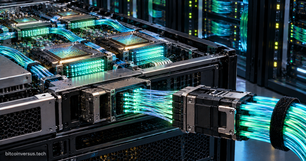
Avicena used ECOC 2026 to push that problem into the spotlight. In a September 17 announcement, the company said it would demonstrate a connectorized version of its LightBundle microLED optical interconnect, adding a detachable inline interface to a short-reach optical link designed for AI scale-in and scale-up.
The technical distinction matters. Optical interconnect research often focuses on bandwidth density, reach, and energy per bit. Avicena is now emphasizing an operational question too: can the optical path be disconnected, reconnected, tested independently, routed through a system, and replaced without treating the entire assembly as one permanent package?
A September 21 X post from Fuelmeup captured the broader ECOC theme, placing Avicena’s connectorized microLED link alongside 1.6T and other high-density optical systems targeting the AI interconnect bottleneck.
The Connector Is the New Part of the Story
Avicena’s LightBundle architecture is built around large numbers of relatively low-speed microLED channels operating in parallel through multicore fiber. Its recent 1 Tbps evaluation kits use as many as 335 channels running at up to 3 Gbps each.
That is different from the usual race to push each individual electrical or optical lane to ever-higher signaling rates. LightBundle instead spreads aggregate bandwidth across many optical emitters and photodetectors.
The ECOC implementation adds a detachable optical interface between those endpoints. According to independent coverage from Semiconductor Today, Avicena demonstrated a reconnectable microLED optical path built around its high-density transceiver technology and multicore fiber.
That may sound less dramatic than another record-setting throughput number, but it addresses a practical issue. AI systems have to be manufactured, qualified, transported, installed, upgraded, and repaired.
Optics Has to Become Maintainable
If optical I/O keeps moving deeper into servers and accelerator trays, maintainability becomes part of the architecture. A permanently attached optical path can be efficient, but it can complicate manufacturing and field replacement if technicians cannot isolate the optical section from the rest of the system.
A detachable interface allows system builders to test electronics and optics separately. It can also make routing easier inside a rack because the optical assembly does not have to remain attached during every manufacturing stage.
That operational logic connects directly to BitcoinVersus.Tech’s coverage of cabling becoming more valuable and more complex inside AI data centers. As optical density rises, the physical layer has to remain serviceable enough for technicians to inspect, clean, test, route, and replace it.
MicroLEDs Attack a Different Part of the Optical Stack
Conventional high-speed optical links often use several components to move data over distance at high per-lane rates. Avicena is targeting shorter AI interconnect distances with a different tradeoff.
MicroLED emitters can switch quickly while consuming little energy, and Avicena’s short-reach architecture uses many channels in parallel rather than concentrating the entire bandwidth into a small number of extremely fast lanes.
That makes the technology relevant to scale-up networks, chip-to-chip connections, accelerator-to-memory paths, and other short links where power and shoreline density can matter as much as reach.
The broader optical market is attacking the same AI problem from multiple directions. BitcoinVersus.Tech recently covered Ciena’s path from 1.6T coherent optics toward 6.4T co-packaged optics, where optics is being pulled increasingly close to switching silicon.
AI Networks Are Running Out of Comfortable Electrical Distance
The reason so many vendors are moving toward optical I/O is physical. As signaling rates increase, high-speed electrical links consume more power and become harder to maintain over distance. Equalization, retimers, larger traces, and more complex signal conditioning can extend electrical reach, but they add their own energy and design costs.
Fiber moves that boundary outward. The challenge is making optical hardware dense and efficient enough that it can enter places where electrical links historically dominated.
This is happening at the same time Ethernet itself moves to higher rates. BitcoinVersus.Tech has tracked 1.6T Ethernet moving closer to data center deployment, increasing the pressure on transceivers, connectors, fibers, switches, and internal system links.
The Physical Layer Has to Scale Too
Avicena’s many-lane strategy also raises a cabling challenge. When hundreds of optical paths are concentrated into a compact interface, alignment, connector design, cleanliness, routing, and manufacturing tolerances become critical.
That is why the connectorized eKit is more than a convenience feature. A deployable AI interconnect has to survive repeated assembly and service while remaining straightforward enough for system manufacturers and technicians to work with.
The Winning Optical Technology Has to Survive the Data Center
AI infrastructure will not be decided by laboratory efficiency alone. Technologies also have to fit manufacturing, rack, service, and field-replacement workflows.
That is the significance of Avicena putting a detachable connector into the LightBundle demonstration. It moves microLED optical I/O one step closer to something system builders can integrate into real hardware.
The remaining questions are commercial and engineering ones: reliability over repeated mating cycles, manufacturing yield, connector cleanliness, packaging cost, production scale, ecosystem support, and how the technology compares with increasingly capable silicon-photonics and co-packaged-optics alternatives.
But the direction is clear. As AI systems consume more bandwidth, optics is moving closer to compute. And as optics moves closer to compute, it has to become as practical to service as the rest of the rack.
Editor’s Note
We volunteer daily to ensure the credibility of the information on this platform is Verifiably True. If you would like to support our research initiatives, please donate here: 3C9o19EH5HSiwEPyCTmEKzxhNCbo2X6TTb
BitcoinVersus.tech is not a financial advisor. This media platform reports on financial subjects purely for informational purposes.


Leave a Reply