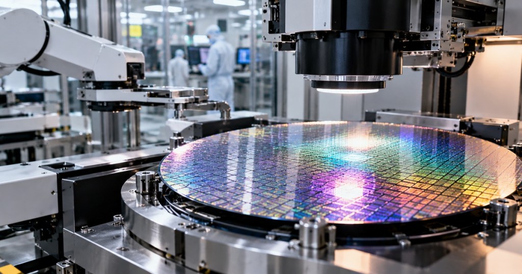
Wafer yield is the percentage of chips on a semiconductor wafer that work well enough to be sold. It sounds like a simple manufacturing statistic, but yield is one of the biggest reasons two chips made with similar equipment can have very different costs.
A wafer can contain hundreds or even thousands of individual chip dies. If most of those dies pass electrical testing, the wafer has high yield. If many fail because of defects, process variation, contamination, or patterning errors, the usable output from the same wafer drops sharply.
Yield Is The Share Of Good Dies
The simplest version of wafer yield can be written as:
Yield = Good Dies ÷ Total DiesIf a wafer contains 600 testable dies and 510 pass, the simple yield is 85%. The remaining 90 dies may fail because of manufacturing defects, electrical problems, or performance that falls outside the product specification.
Why Yield Changes Chip Cost
A semiconductor fab spends money processing the entire wafer, not only the dies that eventually pass. Lithography, deposition, etching, ion implantation, cleaning, metrology, inspection, and other steps are performed across the wafer before final electrical testing separates good dies from bad ones.
If 500 chips can be sold from a wafer instead of 300, much more of the wafer-processing cost is spread across revenue-producing parts. That is why improving yield can reduce effective cost per good chip even when the process equipment, wafer size, and nominal node remain the same.
Defect Density Matters More As Dies Get Larger
A random defect only ruins a die if it lands in a critical area. Larger dies occupy more wafer area, so each individual die has a greater chance of intersecting a defect than a smaller die made with the same defect density.
This is one reason very large CPUs, GPUs, and accelerators can be expensive. Large die area not only means fewer dies fit on the wafer; it can also make the design more sensitive to defects. Chipmakers use inspection and process control to identify defect sources and push the number of working dies upward.
Metrology Helps Fabs Protect Yield
ASML explains that optical metrology and e-beam inspection are used to check printed wafer features, locate defects, and feed measurement data back into the manufacturing process. The goal is not merely to find bad chips at the end; it is to catch process drift early enough to prevent more wafers from being affected.
That feedback loop is important because advanced semiconductor manufacturing contains many repeated patterning and material-processing steps. Small changes in overlay, focus, film thickness, contamination, or critical dimensions can create systematic yield loss across many dies at once.
Not Every Defect Has The Same Impact
Some defects are harmless because they appear in noncritical areas. Others can short two features together, open a connection, distort a transistor structure, or move a key dimension outside the allowed process window.
KLA describes yield management as a process of finding defects, determining which manufacturing problems caused them, taking corrective action, and then monitoring later wafers to confirm the issue has been contained.
A Wafer Map Shows Where Problems Appear
After testing, engineers can plot pass and fail results across the wafer. That wafer map is often more useful than a single yield percentage because the location of failures can reveal the type of problem.
Random isolated failures may point toward particle defects. A ring near the wafer edge, repeated clusters, or a pattern concentrated in one region can suggest equipment, process, temperature, coating, or alignment issues. Yield engineering is therefore partly statistics and partly pattern recognition.
Yield Usually Improves During A Process Ramp
New semiconductor processes rarely begin at mature production efficiency. Early lots help engineers discover weak process steps, adjust recipes, improve tool matching, refine inspection, and remove recurring defect sources.
That gradual improvement is often called yield learning. A process can technically manufacture working chips long before it becomes economical enough for large-scale production. This helps explain why a company may announce a new node or product before volume output reaches its mature cost structure.
Binning Can Recover Partially Good Dies
Not every die has to perform identically to create revenue. Semiconductor companies frequently test chips and sort them into performance or feature categories called bins.
A die that cannot meet the highest clock speed or has a disabled functional block may still qualify as a lower-tier product. That approach can improve the economic value recovered from a wafer even though the chips are not all sold as the same model.
Packaging Changes The Economics Too
Modern chips increasingly combine multiple dies instead of relying on one enormous monolithic die. Our 2D vs. 3D semiconductor packaging guide explains how dies can be connected through advanced packaging instead of being built as one giant piece of silicon.
That can change yield economics because smaller dies may be easier to manufacture with high yield, then assembled into a larger system. Our homogeneous vs. heterogeneous integration explainer shows how chipmakers combine different die types and process technologies inside one package.
Yield Is Why Manufacturing Headlines Need Context
A process node entering production does not automatically mean every wafer is producing mature volumes of sellable chips. Ramp speed, defect density, process stability, die size, packaging, and test results all influence how much useful output actually reaches customers.
That is why our coverage of CXMT’s fifth-generation DRAM production treated manufacturing, process control, and yield maintenance as part of the same story rather than focusing only on a node label.
The Easy Way To Remember It
A wafer is valuable because of the good dies it produces, not simply because it was processed successfully. High yield means more usable chips come from the same manufacturing effort. Low yield means more of that expensive wafer ends up as scrap or lower-value product.
That is why defect inspection, metrology, process control, testing, binning, and packaging all connect back to the same goal: getting as much reliable silicon value as possible from every wafer.
BitcoinVersus.Tech
Advertisement
Editor’s Note
We volunteer daily to help keep the information on this platform verifiably accurate. If you would like to support our independent research, please donate here: 3C9o19EH5HSiwEPyCTmEKzxhNCbo2X6TTb
BitcoinVersus.tech is not a financial advisor. Content is provided for informational purposes.


Leave a comment