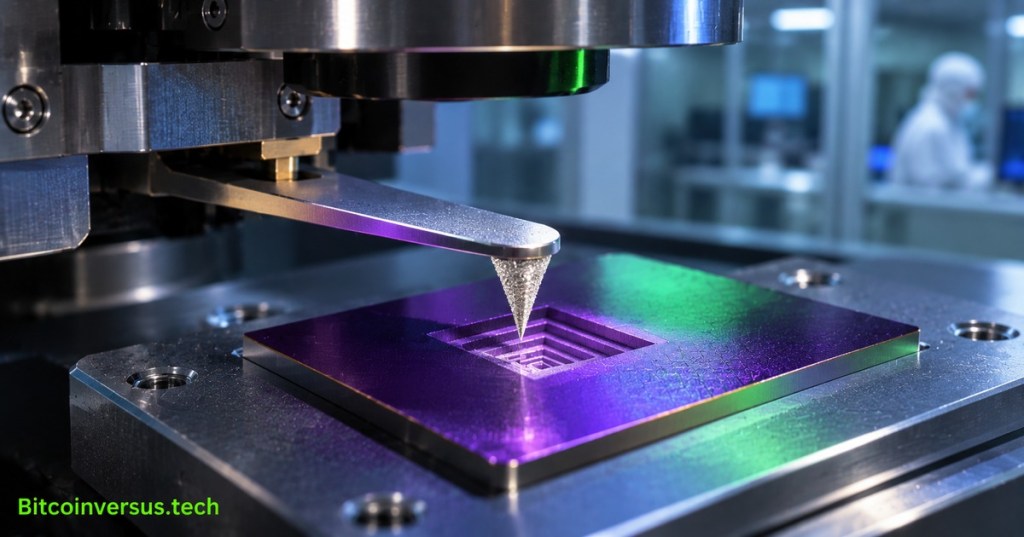
Researchers at South Korea’s Yonsei University have tested a way to control atomic force microscope (AFM) etching of thin films used in emerging semiconductor memory. A peer-reviewed study published November 3, 2026 reports four successive etched layers measuring 7.5, 4.0, 4.1 and 1.9 nanometers, against a nominal target of 5 nanometers per layer. The measurements show both the promise and the variability of nanoscale material removal.
AFM ordinarily maps surface topography by monitoring forces on a sharp probe. Specialized contact-mode techniques can deliberately scratch away material; another imaging scan then checks the exposed layer. Alternating removal and observation enables depth-resolved tomography, unlike a conventional single surface-height map. The distinction matters: etch-based AFM tomography is destructive, even when its verification scan uses noncontact imaging. BitcoinVersus.Tech’s AFM technical reference explains normal height-mapping and measurement limitations.
Three memory materials show different wear responses
Scientists Siwon Park, Young-Min Kim and Jong-Souk Yeo prepared approximately 50-nm-thick amorphous germanium–tellurium (Ge–Te), silicon–tellurium (Si–Te) and germanium–selenium (Ge–Se) films. Using diamond-coated AFM probes, they scanned 5 × 5 micrometer regions at nominal loads from 1,200 to 2,200 nanonewtons, collecting three repetitions at each load. Noncontact scans measured the etched depth afterward.
The paper fitted a composite wear parameter Wᵣ combining wear coefficient and effective hardness. In the 1,800–2,200 nN range, fitted values were 4.94 ± 0.44 for Ge–Te, 3.62 ± 0.14 for Si–Te and 1.69 ± 0.02 for Ge–Se, each in units of 10⁻¹⁰ m²/N. The Ge–Te parameter was approximately 2.92 times Ge–Se’s (4.94 ÷ 1.69) under the study conditions. The figures represent a fitted material-removal parameter, not direct hardness, transistor speed or manufacturing yield.
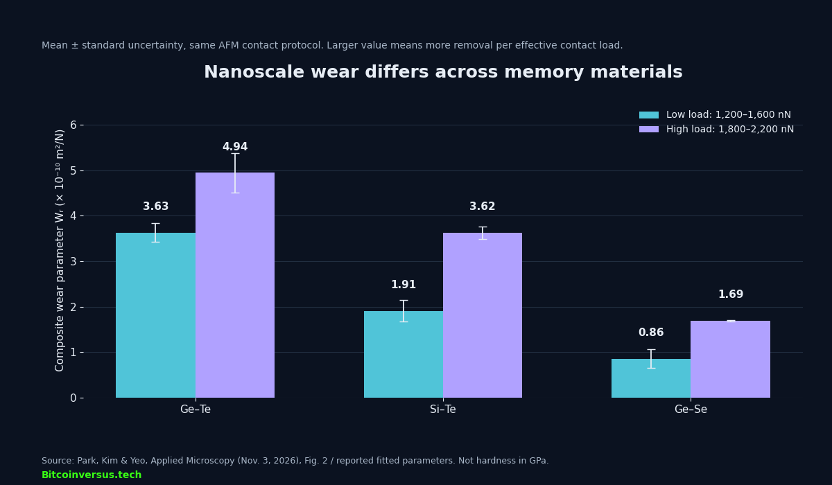
Raman spectroscopy provided another way to rank the film networks: the researchers calculated effective bond-enthalpy descriptors of 223, 333 and 394 kJ/mol for Ge–Te, Si–Te and Ge–Se, respectively. Higher modeled bond-network strength corresponded to less wear under matching contact conditions. The Raman-derived numbers are approximate compositional descriptors, not independently measured absolute bond energies.
A five-nanometer target reveals the remaining gap
The team then used its wear model to choose a 350 nN contact load for a separate Si–Ge–Te film, aiming to remove around 5 nm per pass across a 2.5 × 2.5 micrometer area. Four passes yielded the reported 7.5, 4.0, 4.1 and 1.9 nm. Their arithmetic average is approximately 4.4 nm, around 12% below the planned depth. The total reported cumulative etch depth reached 17.55 nm. Each pass used the same region and probe; the four layers are not independent experimental replicates.
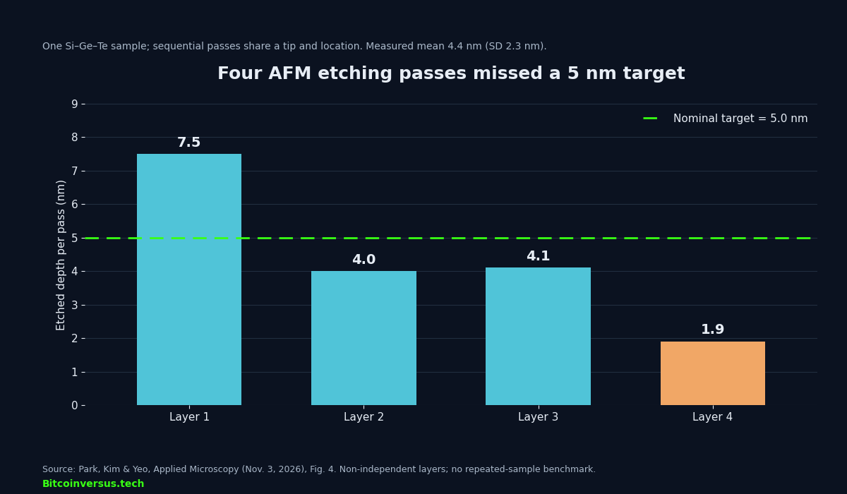
The study reports roughness increasing from 3.58 to 4.41 nm as material accumulated near the etch-groove sides. Probe pull-off forces also changed after etching, complicating comparisons because tip wear and contamination could not be separated. The authors describe their ternary-film experiment as an initial test, not a validated production recipe.
Why memory-chip researchers care
Chalcogenide materials are candidates for phase-change memory and threshold-switching selectors. Their electrical characteristics can depend on local composition and structure, making controlled, depth-resolved analysis valuable. A semiconductor metrology overview explains the broader role of measurement in process control; wafer-yield engineering explains why a laboratory material result alone cannot establish good-die improvements.
Commercial applications remain conditional on repeatability across probes and compositions, calibrated load control, independent specimen trials and acceptable analysis time. Related industry efforts such as eight-head AFM wafer inspection tackle a separate problem: parallelizing measurements rather than controlling how much material a probe removes. Further research must test whether the new predictive approach remains accurate beyond the four-layer proof of concept.
Primary source: Park, Kim and Yeo, Applied Microscopy, November 3, 2026, DOI 10.1186/s42649-026-00147-5. Method context: NIST nanoscale AFM property measurements and Bruker AFM nanolithography techniques.
Editor’s Note: The November 3, 2026 peer-reviewed results concern controlled AFM-based etching of prepared amorphous chalcogenide films in a laboratory. The 5 nm value is a modeled target, not a certified achieved resolution. Four sequential passes were performed on one ternary-film region with the same probe, so they are not independent validation samples. Ge–Te, Si–Te and Ge–Se wear parameters describe fitted composite quantities under particular contact and probe conditions, not absolute film hardness. The cover is a conceptual visualization, and the two charts are original reconstructions from reported numerical data. No live video playback is claimed.
Support BitcoinVersus.Tech
Support independent reporting with an optional 5,000-satoshi donation by scanning the original approved QR code below. On mobile, open the article on another screen to scan with a compatible Bitcoin wallet, or use a supported scan-from-image function. Verify the payment amount and recipient address before sending.

We volunteer daily to ensure the information on this platform is Verifiably True. If you would like to support the research, please scan QR code.


Leave a Reply