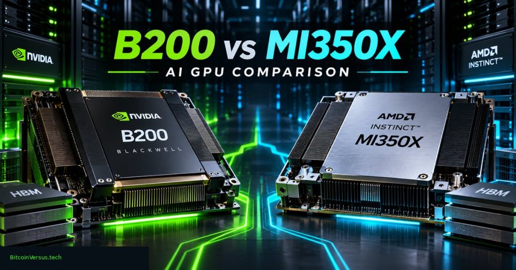
A single AI accelerator can hold only so many model weights and attention-cache entries in its high-bandwidth memory (HBM). When memory runs out, engineers must split a model across processors, move data through an interconnect, or reduce precision. NVIDIA’s B200 Blackwell and AMD’s Instinct MI350X are an informative engineering comparison because both use HBM3E and target large-scale AI training and inference, yet their memory capacities differ substantially. Our GPU-versus-NPU explainer covers their basic computing roles.
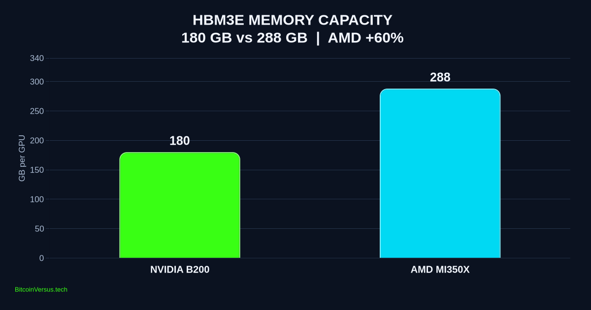
Manufacturer specifications show 288 GB on the MI350X against 180 GB on the B200—a 108 GB, or 60.0%, AMD advantage per device. NVIDIA nevertheless has important ecosystem and interconnect strengths. No independently standardized tokens-per-second test is used in the charts, and neither accelerator is presented as the newest generation available in November 2026.
Memory capacity and bandwidth tell different stories
AMD’s advantage lies in how much data fits locally. The MI350X’s 288 GB can accommodate larger parameter sets or higher key-value-cache allocations before a workload needs sharding. An eight-GPU AMD MI350X platform totals 2,304 GB of listed accelerator memory; the NVIDIA HGX B200 totals 1,440 GB. Those totals multiply eight independent devices, rather than creating one universally accessible contiguous memory pool.
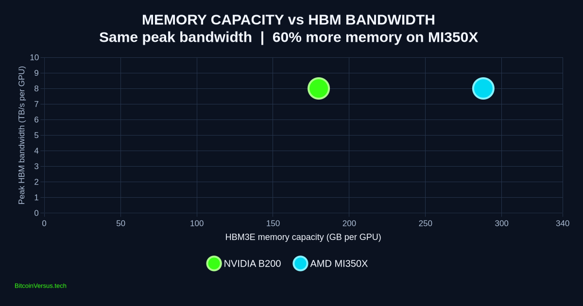
The bandwidth picture is far closer. Both vendors quote up to 8 TB/s of theoretical HBM bandwidth per GPU. Equal peak values do not establish equal sustained throughput: access patterns, kernels, scheduling, memory utilization, and multi-GPU communication can dominate. For broader accelerator positioning, see our Top 7 AI chips overview.
Compute peaks are close, not a measured victory
NVIDIA rates the eight-GPU HGX B200 at 72 PFLOPS FP8/FP6 with sparsity and states that dense performance is half the sparse figure. Dividing 72 by eight GPUs and then by two yields 4.5 PFLOPS per B200. AMD lists 4.6 PFLOPS dense OCP-FP8 matrix performance per MI350X. The arithmetical difference is 0.1 PFLOPS, approximately 2.2% relative to NVIDIA’s quoted value.
However, sparse-versus-dense normalization does not erase differences among FP8-family formats, matrix-engine implementation, numerical requirements, and compiler behavior. A 2.2% gap between marketing ceilings cannot responsibly be called an application-performance win. Our earlier dense-FP8 accelerator ranking explains why chip-level theoretical figures require careful context.
Three defining strengths—and real deployment limits
B200 strengths: 180 GB HBM3E for substantial local AI workloads; up to 8 TB/s memory bandwidth; and fifth-generation NVLink delivering up to 1.8 TB/s bidirectional GPU-to-GPU link bandwidth in supported HGX configurations. NVIDIA’s CUDA software ecosystem is an operational advantage for teams already maintaining CUDA libraries, though no universal productivity percentage can be assigned.
MI350X strengths: 288 GB HBM3E, 8 TB/s peak local bandwidth, and 4.6 PFLOPS published dense OCP-FP8 compute, alongside AMD’s ROCm software stack and open-baseboard integration. Recent ROCm deployment coverage illustrates the ecosystem’s broader engineering ambitions. AMD’s capacity advantage may reduce model partitioning, but real results depend on framework support and workload architecture.
NVIDIA lists B200 GPU power as configurable up to 1,000 W; AMD lists 1,000 W typical board power for MI350X. Maximum configurable consumption and typical board power are different definitions. Neither number establishes equal energy use, cost per token, thermal behavior, or performance per watt. Advanced chip-cooling research reinforces the importance of system-level heat removal.
Verdict: the model and software decide
AMD wins the cleanest directly comparable measure: 60% more HBM capacity per GPU. The two devices tie on published maximum HBM bandwidth, while theoretical FP8-family compute figures remain near one another without proving actual throughput parity. NVIDIA offers a powerful interconnect and mature software workflow; AMD offers larger local memory and a viable alternative software stack. Buyers should benchmark identical models, precisions, latency targets, software versions, rack power, and total cost before naming a system winner.
The two remaining graphics follow our 40-chart visualization framework: zero-based vertical columns for memory capacity and a two-variable scatter plot for memory versus bandwidth. Manufacturer specifications were checked on November 8, 2026. Published peak figures are specifications, not independently repeated measurements under identical server environments.
Editor’s Note: Manufacturer specifications are attributed to their respective vendors. The 4.5-PFLOPS B200 dense figure and 60% memory difference are arithmetic derivations, not independently benchmarked results. The cover is a conceptual AI-generated image, not a photograph of deployed hardware. Two original comparative charts use published figures; workload performance and live system power were not tested.
Support BitcoinVersus.Tech
Independent technology research can be supported with an optional 5,000-satoshi Bitcoin donation. Display the original QR code on another screen and scan it with a compatible wallet, or import a saved image if the wallet supports that method. Verify the recipient and amount before authorizing a payment.

We volunteer daily to ensure the information on this platform is Verifiably True. If you would like to support the research, please scan QR code.


Leave a Reply