AI chips are usually called “the most powerful” without saying what is being measured. This countdown changes the rule: we rank seven major 2026-generation and currently deployed AI accelerators by their published theoretical per-chip, non-sparse FP8 matrix-compute throughput. The unit is petaflops (PFLOPS): quadrillions of floating-point operations per second. These are published hardware ceilings, not measured training speed, tokens per second, benchmark leadership or energy efficiency.
This is a technical companion to BitcoinVersus.Tech’s earlier Top 7 AI Chips in 2026, which ranked hardware by broader impact and software maturity. Here, we use one explicit numerical yardstick. For NVIDIA B300 and AMD MI350-series products, sparsity-enabled marketing numbers are divided out using the manufacturers’ own dense figures; multi-GPU racks are not counted as a single chip.
Important limitation: Not every AI chip vendor publishes a directly usable dense FP8 peak. Google’s newer TPU 8t and TPU 8i, Meta MTIA, and specialized inference chips are not included without directly comparable published FP8 data. Even non-sparse theoretical peaks can differ by supported formats, clocks, memory bottlenecks and actual workloads.
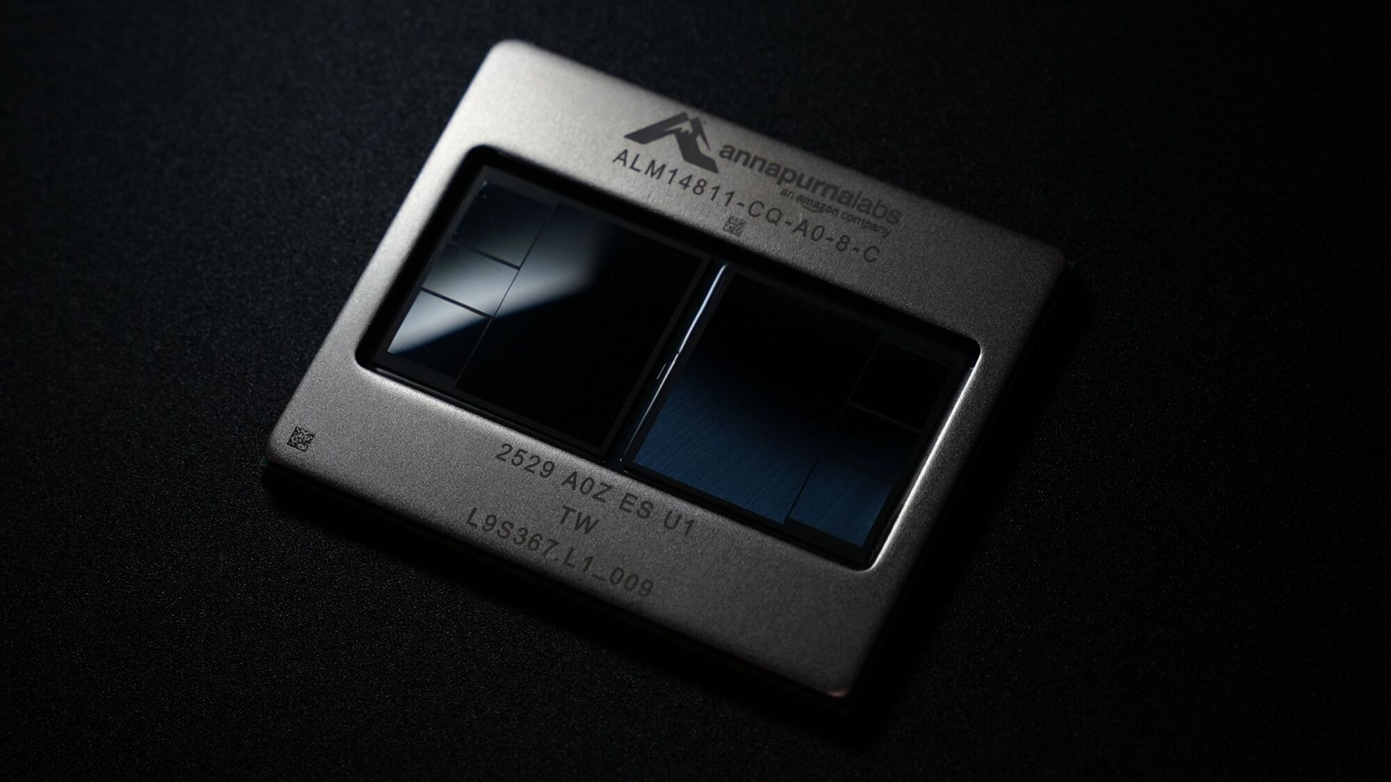
7. AWS Trainium3 — 2.52 PFLOPS FP8 per chip
Amazon Web Services lists 2.52 PFLOPS of FP8 compute for each Trainium3 chip, along with 144 GB of HBM3e and 4.9 TB/s of memory bandwidth. The processor powers EC2 Trn3 UltraServers, which AWS declared generally available on December 2, 2025. This is the smallest quoted FP8 peak in this selected seven-chip comparison, not evidence that Trainium3 is less cost-effective. AWS’s design emphasizes complete cloud-system economics, networking and scale. Primary source: AWS availability announcement and specification. Our Anthropic infrastructure report provides wider investment context.
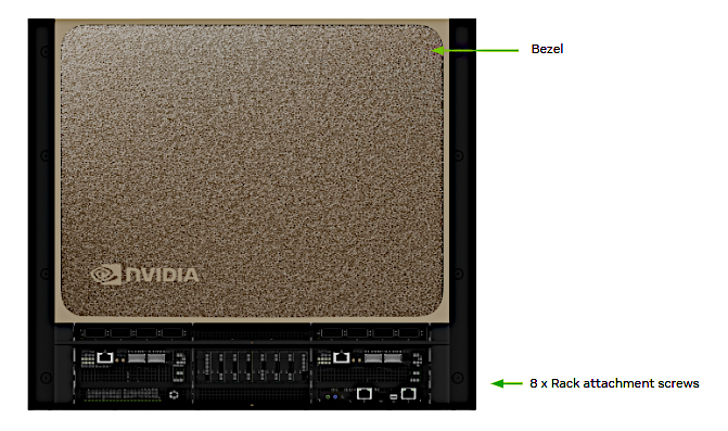
6. NVIDIA Blackwell Ultra B300 — 4.5 PFLOPS dense FP8 per GPU
The eight-GPU HGX B300 platform is rated at 72 PFLOPS FP8/FP6 with sparsity enabled. NVIDIA’s own note states that the dense figure is half of that. Dividing 72 PFLOPS by eight GPUs and then by two gives 4.5 PFLOPS dense FP8 per B300 GPU. This calculation must not be confused with an entire eight-GPU system or the GB300 rack. Blackwell Ultra remains commercially significant because it is shipping, supported by the CUDA stack and paired with high-speed NVLink. For the facility implications, see our coverage of AI chip cooling under rising heat loads.
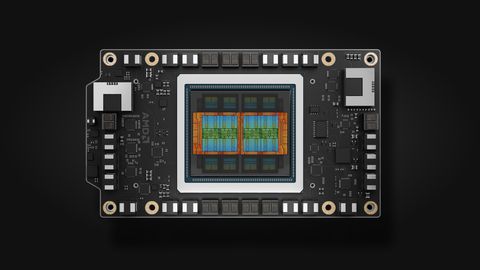
5. AMD Instinct MI350X — 4.6 PFLOPS dense FP8
AMD reports 4.6 PFLOPS non-sparse OCP-FP8 on each MI350X accelerator, compared with 9.2 PFLOPS when structured sparsity is enabled. A single MI350X also offers 288 GB of HBM3e and up to 8 TB/s of HBM bandwidth. It ranks only narrowly ahead of B300 on this one computed metric; a difference of 0.1 PFLOPS should not be interpreted as a meaningful lead in real application performance. Primary source: AMD MI350X product specifications. AMD’s ROCm environment, system layout and model compatibility remain central when choosing a deployment.
4. Google Ironwood TPU7x — 4.614 PFLOPS FP8
Google’s seventh-generation Ironwood TPU delivers a published 4,614 TFLOPS, or 4.614 PFLOPS FP8 per chip. Google’s technical reference also lists 192 GiB of HBM and 7,380 GB/s bandwidth. That puts Ironwood slightly above the rounded MI350X figure here, but the published values are effectively close. Its real strategic strength lies in Google’s pod-scale integration, including configurations of up to 9,216 chips. Primary source: Google Cloud TPU7x specifications.
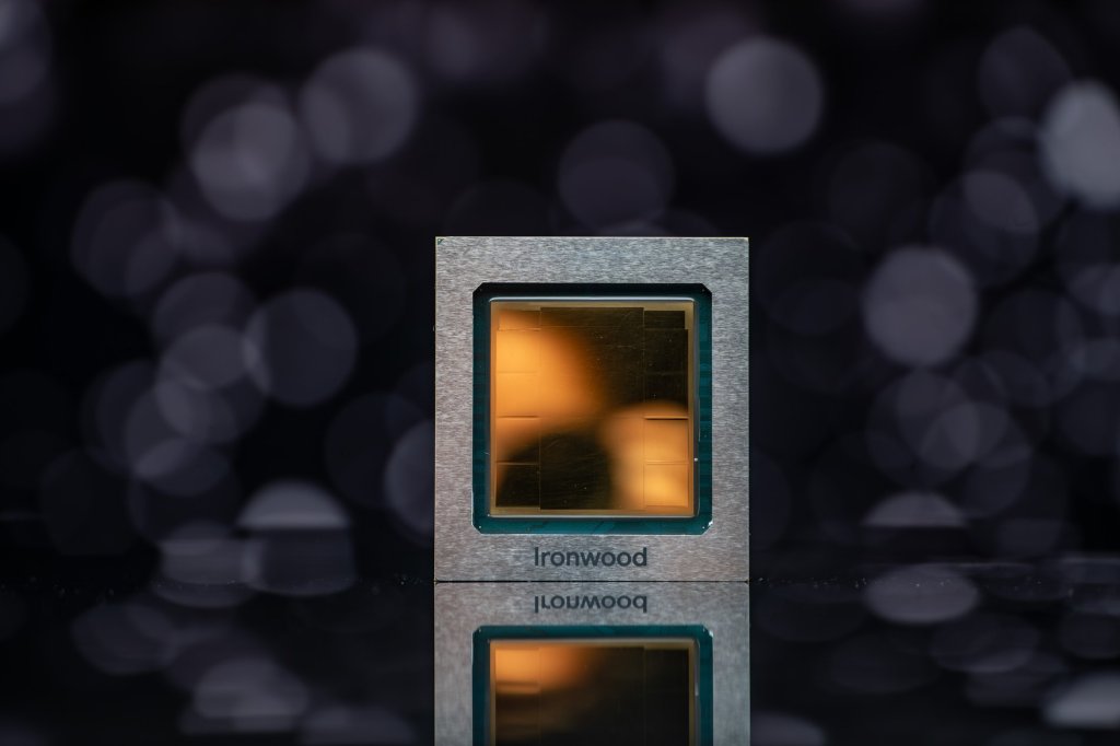
The official Ironwood image shows the actual Google hardware rather than an invented circuit illustration. Google’s launch presentation below explains the TPU’s inference-oriented design and how Google approaches large-scale AI clusters.
Google has since announced TPU 8t and TPU 8i, with 12.6 PFLOPS and 10.1 PFLOPS of FP4 compute respectively, but those FP4 figures cannot simply be relabeled FP8 for this ranking. Google’s own architecture deep dive explains why the chips pursue different training and inference targets.
3. AMD Instinct MI355X — 5.0 PFLOPS dense FP8
The MI355X’s specification distinguishes between 5.0 PFLOPS non-sparse OCP-FP8 and 10.1 PFLOPS with structured sparsity. Its 288 GB of HBM3e, rated at 8 TB/s, gives large models substantial local working memory. MI355X is already part of AMD’s established MI350-series accelerator lineup and makes a useful baseline for the much higher theoretical peak of MI455X. Primary source: AMD MI355X specifications. Its footprint also demonstrates why comparing chips requires consideration of electrical power, coolant distribution, storage and interconnect, not FLOPS alone.
2. NVIDIA Rubin GPU — 17.5 PFLOPS dense FP8
NVIDIA publishes 17.5 PFLOPS FP8/FP6 training compute per individual Rubin GPU, with the specification explicitly marked as dense, not sparse. Each Rubin GPU has 288 GB HBM4 and 22 TB/s memory bandwidth in NVIDIA’s HGX specifications. The chip powers the Vera Rubin platform, and NVIDIA said in March that its component family had entered full production. On October 27, NVIDIA and Oracle announced general availability of Vera Rubin NVL72 on Oracle Cloud Infrastructure. This is an important deployment milestone, though it does not itself validate every theoretical chip specification under real workloads.
NVIDIA’s official GTC keynote provides the original Rubin platform introduction. For a separate physical-infrastructure perspective, read our comparison of NVIDIA DSX POD deployments and Bitcoin mining containers.
A 72-GPU Vera Rubin NVL72 rack is a system rather than a single chip, so its aggregate throughput is not substituted for the one-GPU value shown above. NVIDIA HGX primary specification table provides the per-GPU basis.
1. AMD Instinct MI455X — 20.1 PFLOPS quoted FP8
AMD lists 20.1 PFLOPS peak OCP FP8 per MI455X accelerator, the highest explicitly quoted non-sparse FP8 figure among the seven chips selected here. Introduced in July 2026, MI455X pairs CDNA 5 compute architecture with 432 GB of HBM4 and up to 23.3 TB/s memory bandwidth. AMD’s Helios reference design combines 72 MI455X GPUs, but this ranking deliberately uses one accelerator’s published performance rather than 72 times the figure. Primary source: AMD MI455X specifications; AMD’s July 23 Helios announcement.
AMD’s lead on this specific advertised number is not proof that MI455X processes more useful tokens per watt or delivers faster completion times than Rubin. The real answer depends on dtype implementation, model architecture, software, networking and power. The MI455X family also connects to our coverage of HBM4 supply and Helios liquid-cooling infrastructure.
The ranking covers public company specification sheets as of October 27, 2026. It is a comparison of published peaks, not a lab benchmark. Actual workloads should be tested against memory use, throughput, latency, interconnect bandwidth, energy consumption and ownership costs. For a broader historical comparison of computing hardware, see how supercomputers reached exascale.
What the FP8 race means for the data center
The gap between quoted performance and useful production work is especially important to data-center operators. Dense 8-bit peaks measure a narrow slice of hardware capability; not every model can use FP8 identically, and memory pressure or networking may dominate. From an infrastructure perspective, FP8 throughput must be evaluated alongside liquid-cooling requirements, rack density, HBM availability and the number of meaningful model tokens generated per kilowatt-hour. The next frontier is not simply more FLOPS—it’s more reliable, useful computing delivered within real power and cooling limits.
Editor’s Note: BitcoinVersus.Tech distinguishes verified manufacturer specifications, computed dense equivalents, and real-world performance. Support independent technology research with a donation of 5,000 sats using the QR code below.

Scan the QR code with your Bitcoin wallet camera, ideally while viewing this article on a separate display.


Leave a Reply