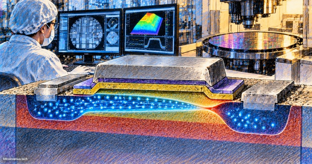
From MOS Capacitor To MOSFET
The MOSFET takes the electrostatics of the MOS capacitor and adds two heavily doped regions called source and drain. In an ideal long-channel NMOS device on a p-type body, a sufficiently positive gate voltage creates an electron inversion layer under the oxide. That inversion layer becomes a controllable channel connecting source to drain. The gate therefore controls whether carriers can move laterally through the semiconductor without requiring steady DC gate current through the oxide.
This lesson focuses on the ideal long-channel device: channel formation, the linear region, pinch-off, saturation, and the square-law current model. Short-channel effects such as velocity saturation, DIBL, and strong channel-length modulation belong to the next stage of the track.
Threshold Voltage Creates The Channel
When the gate-to-source voltage VGS is below the threshold voltage VT, the surface is not in strong inversion and the ideal strong-inversion drain current model does not apply. Once VGS exceeds VT, the gate attracts enough electrons to form a conducting inversion channel between source and drain.
The quantity VOV = VGS − VT is called the overdrive voltage. It measures how far the gate bias is above threshold. In the ideal long-channel model, larger overdrive produces more inversion charge, lower channel resistance in the linear region, and larger drain current in saturation. The underlying carrier motion still depends on the mobility and drift physics developed in OSSEC.002.
A Small Drain Voltage Makes The MOSFET Look Resistive
After the inversion channel forms, applying a small positive VDS creates an electric field from drain to source. Electrons drift from source toward drain, producing conventional drain current in the opposite direction. For a sufficiently small drain voltage, the inversion layer exists along the full channel length and the device behaves approximately like a gate-controlled resistor.
Under the gradual-channel approximation, the ideal NMOS current in this linear or triode region is ID = μnC′ox(W/L)[(VGS−VT)VDS − VDS2/2]. Here μn is electron mobility, C′ox is oxide capacitance per unit area, W is channel width, and L is channel length. The equation shows why wider devices conduct more current while longer channels conduct less.
The Channel Is Not Uniform From Source To Drain
The local inversion charge depends on the difference between gate voltage and the local channel potential. Near the source, the channel potential is close to the source voltage, so gate control is strongest. Moving toward the drain, channel potential rises and the effective gate-to-channel voltage falls. The inversion sheet therefore becomes progressively thinner toward the drain as VDS increases.
This is the key physical idea behind pinch-off. The MOSFET does not have one uniform channel charge from source to drain. The drain voltage reshapes the channel because the gate is controlling a surface whose electrical potential changes along its length.
Pinch-Off Starts When VDS Reaches The Overdrive Voltage
At the drain end, inversion charge approaches zero when the local gate-to-channel voltage falls to approximately threshold. In the ideal long-channel model, this occurs when VDS ≈ VGS − VT = VOV. This condition is called pinch-off.
Pinch-off does not mean current becomes zero. Electrons still travel through the inversion channel, enter the high-field region near the drain, and are swept into the drain. The important change is that increasing VDS no longer creates a proportional increase in channel inversion charge along the full device. That is why the output characteristic transitions from a resistor-like slope toward saturation.
Saturation Produces The Ideal Square Law
For the ideal long-channel NMOS, saturation begins when VDS ≥ VOV. Ignoring channel-length modulation, the drain current becomes approximately independent of further VDS increase and is given by ID,sat = ½ μnC′ox(W/L)(VGS−VT)2.
This is the classic MOSFET square law. Doubling ideal overdrive voltage increases the modeled saturation current by a factor of four, provided the assumptions remain valid. The model is extremely useful for understanding device physics and circuit behavior even though deeply scaled modern transistors depart from the simple square law.
Transconductance Measures Gate Control Over Current
Transconductance gm measures how strongly drain current changes when gate voltage changes. In ideal long-channel saturation, differentiating the square-law equation gives gm = μnC′ox(W/L)VOV. The same result can be written as gm = 2ID/VOV.
That relationship is important because it connects device physics to analog gain. A MOSFET with higher inversion charge, larger width, higher mobility, or stronger gate capacitance can produce a larger current response to a small change in gate voltage. Real devices also include parasitic source and drain series resistance, which can reduce the effective voltage actually applied to the intrinsic transistor.
Read ID–VD And ID–VG Curves Together
An ID–VD family of curves shows how drain current changes with drain voltage at several gate voltages. Each curve begins in the linear region and bends toward saturation near VDS ≈ VOV. An ID–VG curve instead shows how gate voltage creates channel charge and increases current at a chosen drain bias. Engineers use both views because one exposes output behavior while the other exposes gate control and threshold behavior.
The definition of threshold extracted from measured I–V data can depend on method, device geometry, bias, and non-idealities. That is why threshold-voltage extraction should not be confused with one perfectly universal physical point.
Worked Example
- Given: μnC′ox(W/L) = 1 mA/V², VT = 0.5 V, and VGS = 1.5 V.
- Overdrive: VOV = 1.5 − 0.5 = 1.0 V.
- Saturation boundary: VDS,sat ≈ 1.0 V.
- Ideal saturation current: ID,sat = ½(1 mA/V²)(1.0 V)² = 0.5 mA.
- Ideal transconductance: gm = 2ID/VOV = 1 mS.
- Physical meaning: the device behaves resistively below the saturation boundary, then approaches the square-law saturation current after pinch-off.
Where The Ideal Model Breaks
The long-channel model intentionally ignores effects that become important in modern devices. Real saturation current often still rises with drain voltage because the effective channel shortens after pinch-off. High lateral electric fields can limit carrier velocity. Strong drain fields can reduce the source-channel barrier. Mobility can degrade as vertical field increases. Contact and series resistance also consume voltage outside the intrinsic channel.
Those departures do not make the ideal model useless. They make it the reference model against which real behavior is understood. The distinction between an ideal device equation and measured transistor behavior is central to semiconductor engineering.
Engineering Checklist
- Identify NMOS or PMOS and choose a consistent voltage sign convention.
- Determine VT and calculate overdrive VOV.
- Check whether a strong-inversion channel should exist.
- Compare VDS with VOV to identify linear or saturation operation.
- Use the linear-region current equation only when VDS is below the ideal saturation boundary.
- Use the square-law saturation equation only under long-channel assumptions.
- Read I–V data for departures from ideal behavior before applying a simple model blindly.
- Account for series resistance, threshold extraction method, temperature, geometry, and process conditions when comparing measurements.
Exercises
- For VGS = 1.2 V and VT = 0.4 V, calculate VOV and the ideal saturation boundary.
- Explain physically why the inversion charge becomes smaller near the drain as VDS increases.
- Explain why pinch-off does not mean drain current stops.
- Using k = μC′ox(W/L) = 2 mA/V² and VOV = 0.5 V, calculate ideal ID,sat.
- Explain why doubling W approximately doubles ideal drain current.
- Explain why doubling L approximately halves ideal current if every other model parameter stays unchanged.
- Describe one reason a measured saturated MOSFET may not show perfectly flat ID versus VDS.
Knowledge Check + Answers
- What creates the NMOS inversion channel? A gate voltage above threshold attracts enough electrons to create strong inversion at the surface.
- What is overdrive voltage? VOV = VGS − VT.
- When is an ideal NMOS in the linear region? When VGS > VT and VDS < VOV.
- When does ideal saturation begin? Approximately when VDS reaches VOV.
- Does pinch-off mean current becomes zero? No. Carriers cross the high-field region near the drain and current continues.
- What is the ideal long-channel saturation relationship? ID,sat is proportional to (VGS − VT)².
- What does transconductance measure? The change in drain current produced by a change in gate voltage.
Prior Lessons And References
- OSSEC.001 — Semiconductor Device Physics
- OSSEC.002 — Carrier Transport
- OSSEC.005 — MOS Capacitor Physics
- Semiconductor Fundamentals — Metal–Oxide–Semiconductor
- MOSFET Operating Characteristics
- The MOSFET Square Law
- MIT OpenCourseWare — MOSFET I–V Lectures
- NPTEL — Introduction to Semiconductor Devices
Elementary Conclusion
An ideal long-channel MOSFET is easiest to understand as a MOS capacitor extended sideways between source and drain. The gate creates the inversion channel, the drain voltage drives carriers through it, the channel charge tapers toward the drain, and pinch-off marks the transition into saturation. The square-law model then connects geometry, mobility, oxide capacitance, threshold voltage, and gate overdrive to drain current. That model is the foundation for understanding both transistor circuits and the non-ideal effects that appear as devices become shorter and faster.
BitcoinVersus.Tech
Advertisement
BitcoinVersus.Tech publishes open technical education across semiconductor engineering, electronics, programming, operating systems, networking, robotics, and data centers.
Editor’s Note
The equations in this lesson describe an ideal long-channel MOSFET under stated assumptions. Real device behavior depends on process technology, geometry, temperature, parasitic resistance, mobility degradation, short-channel effects, and the chosen compact model.
We volunteer daily to help keep the information on this platform verifiably accurate. Support our independent research through the support options available on BitcoinVersus.Tech.
BitcoinVersus.tech is not a financial advisor. Content is provided for informational purposes.


Leave a comment