Why The MOS Capacitor Matters
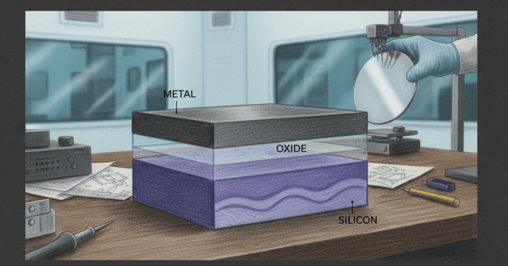
The metal–oxide–semiconductor (MOS) capacitor is the electrostatic core of the MOSFET. Its stack is simple: a conductive gate, a thin insulating oxide, and a semiconductor substrate. The oxide blocks steady DC current while still allowing the gate electric field to rearrange charge near the silicon surface. For a simple parallel-plate approximation, the oxide capacitance is Cox = εoxA/tox, or per unit area C′ox = εox/tox. A thinner oxide therefore produces a larger gate capacitance and stronger electrostatic control. This lesson extends the band-gap and doping physics, carrier transport, and electrostatics developed earlier in the track.
Accumulation Pulls Majority Carriers To The Surface
Consider an NMOS-style capacitor built on p-type silicon. A sufficiently negative gate voltage attracts holes, the majority carriers, toward the oxide–silicon interface. That region is called accumulation. The surface becomes more heavily populated with holes than the neutral bulk, and the small-signal capacitance approaches the oxide capacitance because there is no wide depletion region acting in series with the oxide. The sign reverses for an n-type substrate. Thinking in terms of charge is useful, but the same behavior can also be read from the energy-band bending inherited from semiconductor electrostatics.
Depletion Creates A Second Effective Capacitor
As the gate on a p-type substrate moves positive, holes are repelled from the surface and leave behind fixed ionized acceptors. The resulting space-charge region is depletion. Under the depletion approximation, its width grows roughly as Wd ≈ √(2εsiψs / qNA), where ψs is surface potential and NA is acceptor density. The depletion region has its own capacitance, C′dep = εsi/Wd. The measured MOS capacitance therefore behaves like oxide and depletion capacitances in series: 1/C′ = 1/C′ox + 1/C′dep. This is closely related to the depletion-width and junction-capacitance reasoning used for PN junctions.
Inversion Creates The Future MOSFET Channel
Continue increasing the positive gate voltage and the p-type surface eventually becomes electron-rich. Minority carriers now outnumber holes at the interface, producing an inversion layer. In the strong-inversion picture, the surface potential is commonly approximated as ψs ≈ 2φF, where the magnitude of the bulk Fermi potential for p-type material is φF = (kT/q) ln(NA/ni). The depletion region then approaches a maximum width while additional gate voltage primarily increases inversion charge. Once source and drain regions are added, this controllable electron sheet becomes the conductive channel that defines MOSFET operation.
Threshold Voltage Combines Surface Potential And Oxide Drop
The threshold voltage is the gate voltage associated with the onset of strong inversion. For an ideal NMOS capacitor on p-type silicon, a common engineering form is VT ≈ VFB + 2φF + |Q′d,max|/C′ox. The first term is the flat-band reference, the second supplies the required silicon band bending, and the third is the oxide voltage required to support maximum depletion charge. Real devices shift because of gate work-function differences, oxide charge, interface states, substrate bias, and other non-idealities. That is why threshold-voltage extraction is a measurement problem as well as a theory problem.
The C–V Curve Turns Electrostatics Into A Measurement
A MOS C–V measurement sweeps DC gate bias while applying a small AC signal to measure incremental capacitance. In accumulation, C approaches Cox. In depletion, the widening space-charge region lowers total capacitance. In inversion, the result depends on measurement frequency: at low enough frequency, minority carriers can respond and capacitance may rise again toward Cox; at high frequency, inversion charge cannot follow the AC signal quickly enough, so capacitance stays near a minimum set by oxide and maximum depletion capacitance in series. C–V data can therefore reveal oxide thickness, doping, flat-band behavior, threshold, and signs of oxide charge density or interface problems.
Read Band Diagrams And Charge Together
A reliable MOS analysis uses three views at the same time: gate voltage, charge distribution, and energy bands. Negative gate bias on p-type silicon produces accumulation; modest positive bias produces depletion; larger positive bias bends the bands far enough to create inversion. The Fermi-level and doping concepts from OSSEC.001 explain why carrier concentrations change exponentially with band position, while the carrier-transport framework explains why minority carriers may or may not respond quickly enough during AC measurements. The central engineering habit is to avoid memorizing a C–V curve in isolation: derive what should happen from field direction, charge sign, band bending, and available carriers.
Worked Example
- Given: SiO₂ thickness tox = 10 nm and εox ≈ 3.45 × 10⁻¹¹ F/m.
- Convert thickness: 10 nm = 1.0 × 10⁻⁸ m.
- Oxide capacitance per unit area: C′ox = εox/tox.
- Result: C′ox ≈ 3.45 × 10⁻³ F/m².
- Equivalent: about 3.45 fF/µm².
- Engineering meaning: halving oxide thickness approximately doubles C′ox, strengthening gate electrostatic coupling before quantum and reliability effects are considered.
Exercises
- For a p-type MOS capacitor, state the sign of gate bias that produces accumulation, depletion, and inversion.
- Explain why increasing depletion width lowers measured capacitance.
- Calculate C′ox for SiO₂ with tox = 5 nm using εox = 3.45 × 10⁻¹¹ F/m.
- Explain physically why strong inversion is associated with ψs ≈ 2φF.
- Describe why high-frequency and low-frequency C–V curves differ in inversion.
- Name three non-ideal effects that can shift VFB or VT.
Knowledge Check + Answers
- What is C′ox? Oxide capacitance per unit area, approximately εox/tox.
- What is accumulation? An increase of majority carriers at the semiconductor surface.
- What is depletion? A surface region depleted of mobile majority carriers and containing fixed ionized dopants.
- What is inversion? A surface condition where minority carriers become the dominant mobile carrier type.
- What approximately defines strong inversion for an ideal p-type substrate? ψs ≈ 2φF.
- Why does MOS capacitance fall in depletion? Oxide capacitance and depletion capacitance act in series.
- Why can high-frequency inversion capacitance stay low? Minority carriers cannot respond rapidly enough to the AC test signal.
Prior Lessons And References
- OSSEC.001 — Semiconductor Device Physics
- OSSEC.002 — Carrier Transport
- OSSEC.003 — PN Junction Electrostatics
- OSSEC.004 — Diode Current–Voltage Physics
- MIT OpenCourseWare — Lecture 9: MOS Capacitors I
- NPTEL — Introduction to Semiconductor Devices
BitcoinVersus.Tech
Advertisement
Editor’s Note: MOS capacitor equations depend on device assumptions, sign conventions, material properties, temperature, geometry, and the treatment of interface and oxide charge. Use the exact device model and process parameters for engineering calculations.
We volunteer daily to help ensure the credibility of the information on this platform is Verifiably True. If you would like to support our research initiatives, please donate here: 3C9o19EH5HSiwEPyCTmEKzxhNCbo2X6TTb
BitcoinVersus.tech is not a financial advisor. Content is provided for informational purposes.


Leave a comment