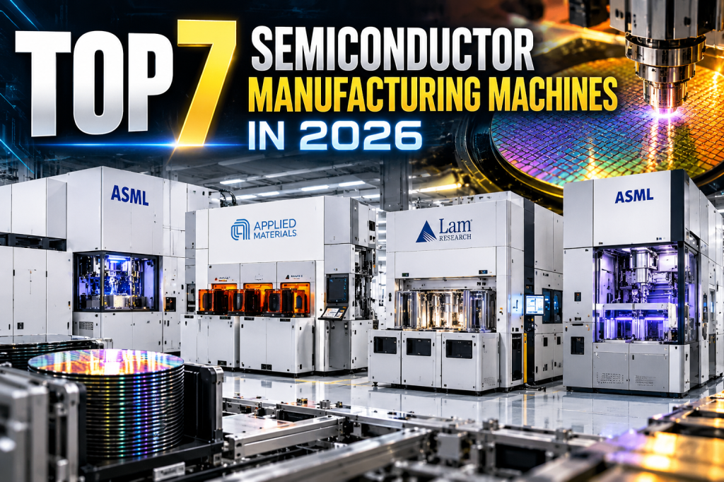
The most advanced chips in 2026 depend on machines that can deposit, etch, measure, bond and print features at atomic or near-atomic scales. This countdown ranks seven semiconductor manufacturing machines by technical importance, production relevance, precision, impact on leading-edge logic and memory, and how strongly each tool shapes the next generation of AI hardware.
This story follows our recent Top 7 AI Chips in 2026, TSMC’s record AI-driven quarter, and AI agents moving into semiconductor fabs.
7. Applied Materials Centura Xtera Epi
Applied Materials’ Centura Xtera Epi is built for selective epitaxial growth in advanced gate-all-around logic and future memory structures. Its chamber architecture is designed to improve precursor delivery and process uniformity while growing silicon-based materials inside increasingly complex three-dimensional transistor structures. Applied says leading foundry customers have already adopted the system for next-generation manufacturing.
Applied Materials demonstrates the Centura Xtera Epi system.
6. Applied Materials PROVision 10
PROVision 10 is an eBeam metrology machine built to measure structures that optical tools increasingly struggle to resolve. Applied Materials says it provides sub-nanometer imaging, can collect up to 100 million actionable measurements per hour, and can see through multiple layers of complex three-dimensional chips. That makes it important for 2 nm logic, gate-all-around transistors, advanced DRAM, HBM and backside-power structures.
Applied Materials introduces PROVision 10 alongside its newest AI-chip manufacturing systems.
5. Applied Materials Centura Sculpta
Centura Sculpta adds a manufacturing step called pattern shaping. Instead of printing an additional EUV mask layer, Sculpta can precisely modify existing wafer features in one direction to tighten spacing and improve pattern fidelity. Applied Materials designed it for critical leading-edge logic layers, where eliminating a lithography-and-etch sequence can reduce process complexity, energy use, water use and manufacturing cost.
Applied Materials explains how Sculpta pattern shaping can replace an EUV double-patterning step.
4. Lam Research Akara
Lam Research Akara is a conductor-etch machine designed for future three-dimensional logic and memory structures. Its DirectDrive solid-state plasma source can respond to process changes more than 100 times faster than previous plasma sources, while Lam’s ion-energy and plasma-pulsing controls target angstrom-level critical-dimension uniformity. The machine is aimed at demanding structures including CFET logic, 3D DRAM and advanced NAND.
Lam Research demonstrates the Akara conductor-etch machine.
3. Applied Materials Kinex
Kinex is an integrated die-to-wafer hybrid-bonding machine developed by Applied Materials with Besi. It combines surface preparation, bonding and in-line metrology so chiplets can be aligned and joined with extremely small interconnect pitches while reducing contamination and queue-time variation. Hybrid bonding is becoming increasingly important for HBM, AI accelerators and other multi-die packages where bandwidth and power efficiency depend on moving dies closer together.
Applied Materials demonstrates the Kinex integrated hybrid-bonding system.
2. ASML TWINSCAN NXE EUV
ASML’s TWINSCAN NXE family remains the workhorse for leading-edge EUV production. The current NXE:3800E generation reached 230 wafers per hour in 2026 after a productivity upgrade, while retaining the 0.33 numerical aperture architecture used to print critical logic and memory layers. These machines remain essential because high-volume chip production requires not only tiny features, but also enormous throughput and repeatable overlay accuracy.
ASML shows the laser-and-tin EUV light source inside a TWINSCAN NXE lithography machine.
1. ASML TWINSCAN EXE:5200B High-NA EUV
ASML TWINSCAN EXE:5200B takes No. 1 because it changes the fundamental resolution available to chipmakers. The 0.55-NA High-NA EUV machine delivers 8 nm resolution and roughly 40 percent higher imaging contrast than the NXE family. ASML says it can print features 1.7 times smaller in a single exposure, enabling transistor densities about 2.9 times higher. In 2026, the second-generation High-NA system was already operating at a customer site as the industry worked toward high-volume manufacturing insertion.
ASML introduces its High-NA EUV TWINSCAN EXE technology.
The most important lesson from this list is that advanced chipmaking is not dominated by lithography alone. EUV machines may define the smallest printable features, but modern chips also require atomic-scale deposition, plasma etching, eBeam measurement, pattern correction and advanced packaging. Every additional generation of AI hardware depends on these machines working together with tighter tolerances and higher throughput.
BitcoinVersus.Tech Editor’s Note:
We volunteer daily to ensure the credibility of the information on this platform is Verifiably True. If you would like to support to help further secure the integrity of our research initiatives, please donate using the QR code provided

For best QR-code scanning results, please scan this donation code from a desktop or larger screen. Mobile screens may prevent camera recognition.


Leave a Reply