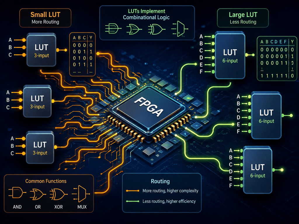
Look-Up Tables (LUTs) are one of the fundamental building blocks used inside Field-Programmable Gate Arrays (FPGAs) to implement digital logic.
A LUT stores predefined output values for every possible combination of its input signals, allowing an FPGA to reproduce Boolean logic functions without requiring a dedicated physical circuit for every operation.
When an FPGA design is synthesized, logic equations written in languages such as Verilog or VHDL are commonly mapped into LUTs distributed throughout the programmable fabric.
The size of a LUT affects both logic capacity and routing requirements. Larger LUTs can accept more input signals and implement more complex combinational functions inside a single logic block, potentially reducing the amount of interconnect required between FPGA resources.
Smaller LUTs may require several LUTs to implement the same function, increasing routing, but they can sometimes use FPGA resources more efficiently when the design contains many relatively simple logic functions. Modern FPGA architectures therefore balance LUT size, routing resources, flip-flops, and configurable logic blocks to improve performance and silicon utilization.
LUTs can implement many forms of combinational digital logic, including AND, OR, XOR, multiplexers, decoders, comparators, and portions of arithmetic circuits. When combined with registers, carry chains, memory resources, DSP blocks, and programmable routing, LUTs help form much larger FPGA systems such as embedded processors, hardware accelerators, communications controllers, and industrial control logic.
Understanding LUT architecture is therefore essential for learning FPGA programming, digital electronics, RTL design, and hardware optimization.


Leave a Reply