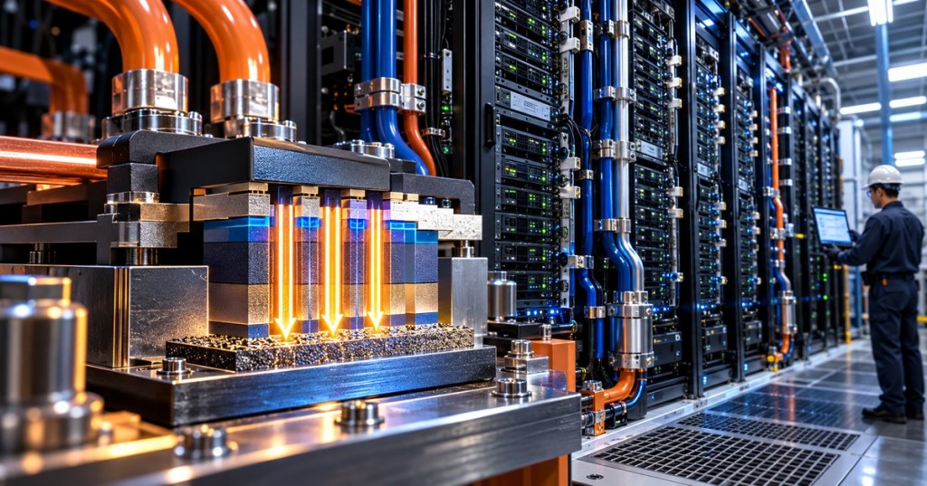
On October 22, 2026, the U.S. Department of Commerce announced a letter of intent for up to $73 million in research funding for Boston-based Vertical Semiconductor. The MIT spinout aims to develop vertical gallium nitride (GaN) power transistors and demonstrate a 2.5-megawatt AI data-center rack. The funding is proposed, not a finalized or disbursed award.
Key Takeaways
- Vertical Semiconductor’s potential $73 million award is part of a broader $389 million federal R&D proposal.
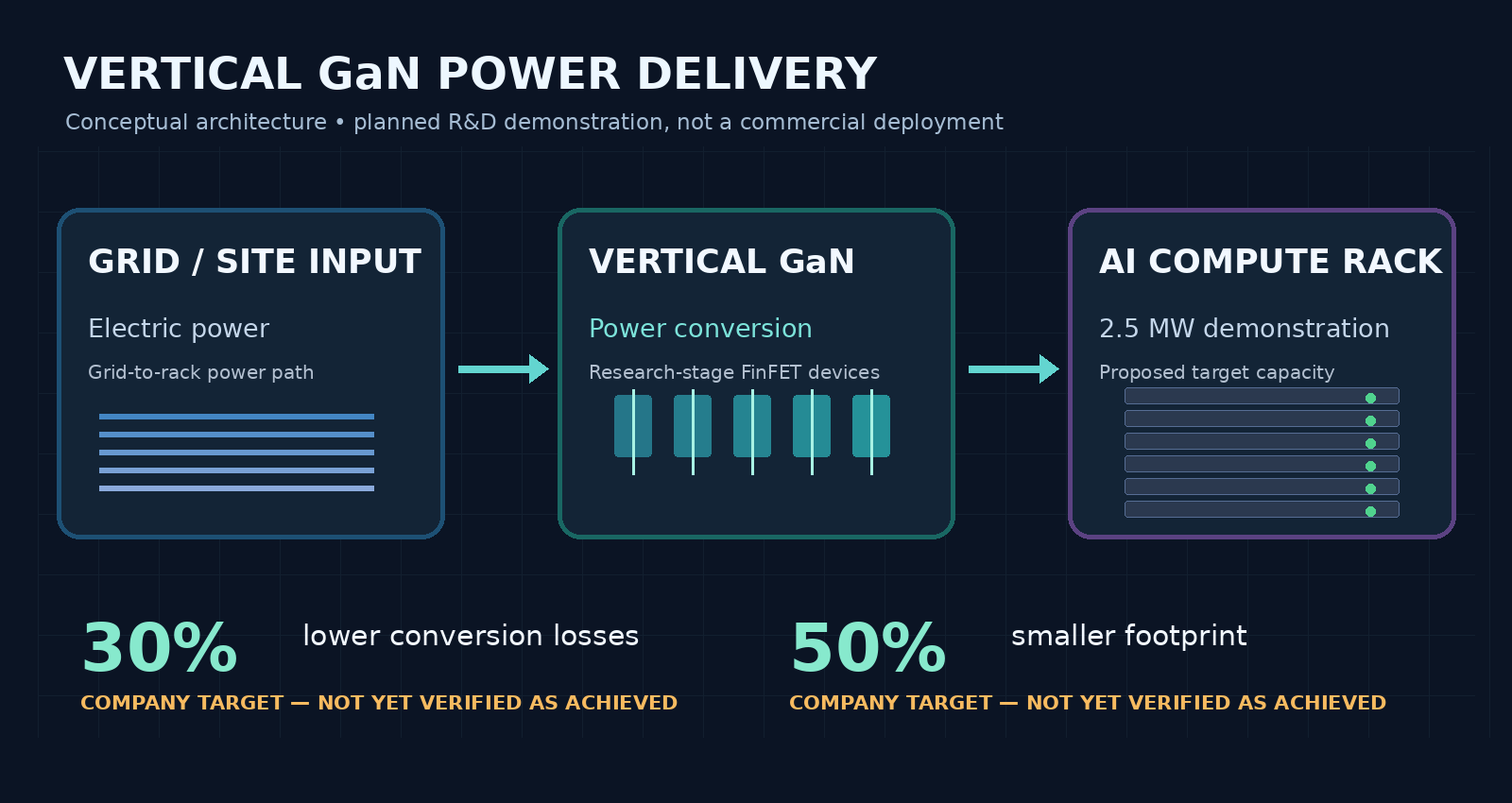
- Its planned 2.5 MW rack is a research demonstration, not an operating installation.
- The company’s targets include 30% lower power-conversion losses and 50% less physical footprint; neither outcome is established by the announcement.
Why Vertical GaN Matters
GaN is a wide-bandgap semiconductor used in high-speed, high-efficiency power switching. In Vertical Semiconductor’s design, current flows through the device vertically rather than primarily across its surface. That geometry could accommodate higher voltages and current density while reducing conversion losses, although practical results depend on device packaging and reliability.
In a September technical interview, CEO Cynthia Liao discussed 8-inch engineered substrates and planned devices rated at 100 V, 650 V and 1,200 V. Our previous coverage of 1,200 V vertical GaN and Renesas power semiconductors explains why higher-density switching matters.
What the Federal Proposal Actually Covers
The Commerce Department announcement lists three other proposed recipients: Helion (up to $175 million), Commonwealth Fusion Systems ($85 million) and Sibelco ($56 million). Each contemplated final award would give the government a minority, non-controlling, non-voting equity stake. The letters of intent do not establish that money has changed hands.
According to Vertical Semiconductor’s announcement, the 2.5 MW demonstration would target 30% lower energy losses and a 50% smaller footprint. Those are proposed engineering goals, not measurements from a commissioned rack. The approach complements wider work on 800 V-to-6 V rack conversion and denser embedded power devices.
What Happens Next
The meaningful milestones are finalized terms, reproducible device testing, manufacturing yield, field reliability and a documented rack-level demonstration. The announcement is evidence of federal interest in AI power delivery—not proof that the advertised efficiency or footprint improvements have already been achieved.
BitcoinVersus.Tech Editor’s Note:
We volunteer daily to ensure the credibility of the information on this platform is Verifiably True. If you would like to support to help further secure the integrity of our research initiatives, please donate using the QR code provided

For best QR-code scanning results, please scan this donation code from a desktop or larger screen. Mobile screens may prevent camera recognition.


Leave a Reply