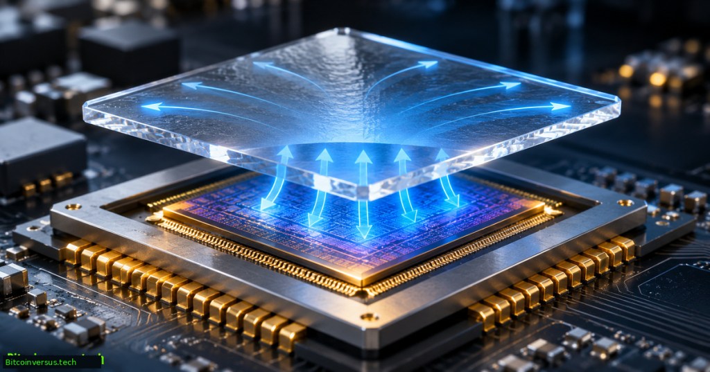
A diamond does not need to come from a mine to be a real diamond. Synthetic diamond has the same underlying crystalline carbon structure as natural diamond, although crystal purity, grain structure and manufacturing method can differ. For heat management, engineers select industrial grades by thermal properties and bonding behavior rather than gemstone appearance.
The answer to a question raised by BitcoinVersus.Tech’s earlier Entegris report is explicit: Element Six and Entegris announced a synthetic-diamond collaboration on November 3, 2026. Both single-crystal and polycrystalline diamond platforms are under consideration for cooling GPUs and radio-frequency devices. Mined stones are not the stated production route.
Synthetic diamond wins the conductivity comparison
Chemical vapor deposition, or CVD, grows diamond from carbon-containing gases on prepared surfaces. Element Six advertises thermal grades spanning approximately 1,000–2,200 watts per meter-kelvin (W/m·K). By comparison, the NIST-hosted reference compilation lists bulk silicon at 148 W/m·K at 300 kelvin, roughly room temperature.
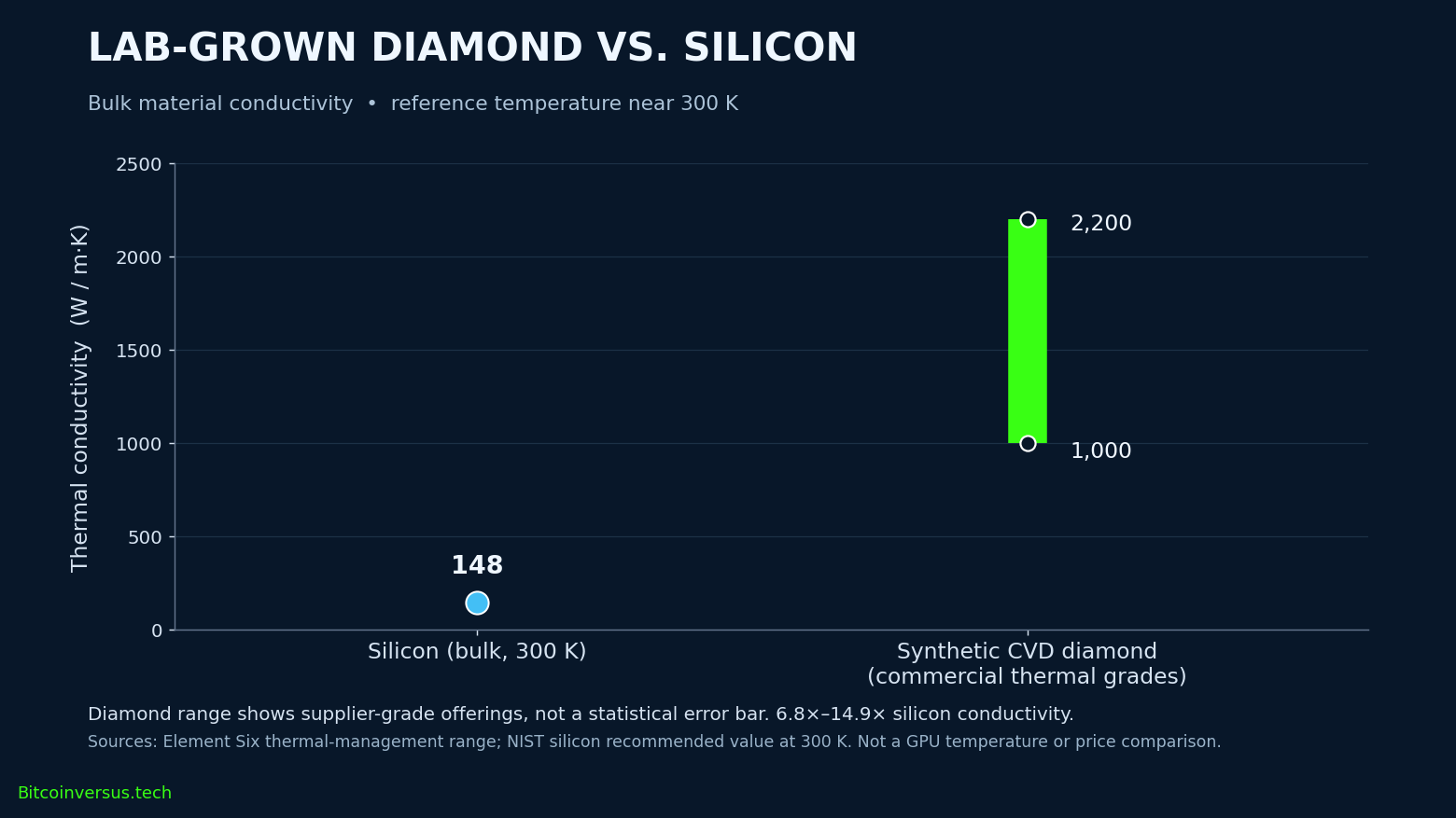
The ratio is approximately 6.8 to 14.9 times for the cited material properties. A GPU will not automatically run 6.8 to 14.9 times cooler: package thickness, die hot spots, contact resistance, heat-spreader area and the cooling loop affect the final junction temperature.
A heat spreader is not a replacement for the silicon wafer
Conventional transistor fabrication begins with a large silicon ingot grown using the Czochralski process. The ingot is shaped, sliced, polished and cleaned before circuits are patterned onto the wafers, as OSHA’s semiconductor process guide describes. Synthetic diamond can instead serve as a heat-spreading or bonded thermal layer added around the functioning silicon device.
Element Six’s June 16 manufacturing update with Orbray reported a reproducible three-inch single-crystal diamond wafer process. Four-inch development was ongoing, and two-inch thermal-bonding wafers were being prepared for volume production. The established silicon industry, by contrast, commonly manufactures on 300-millimeter wafers.
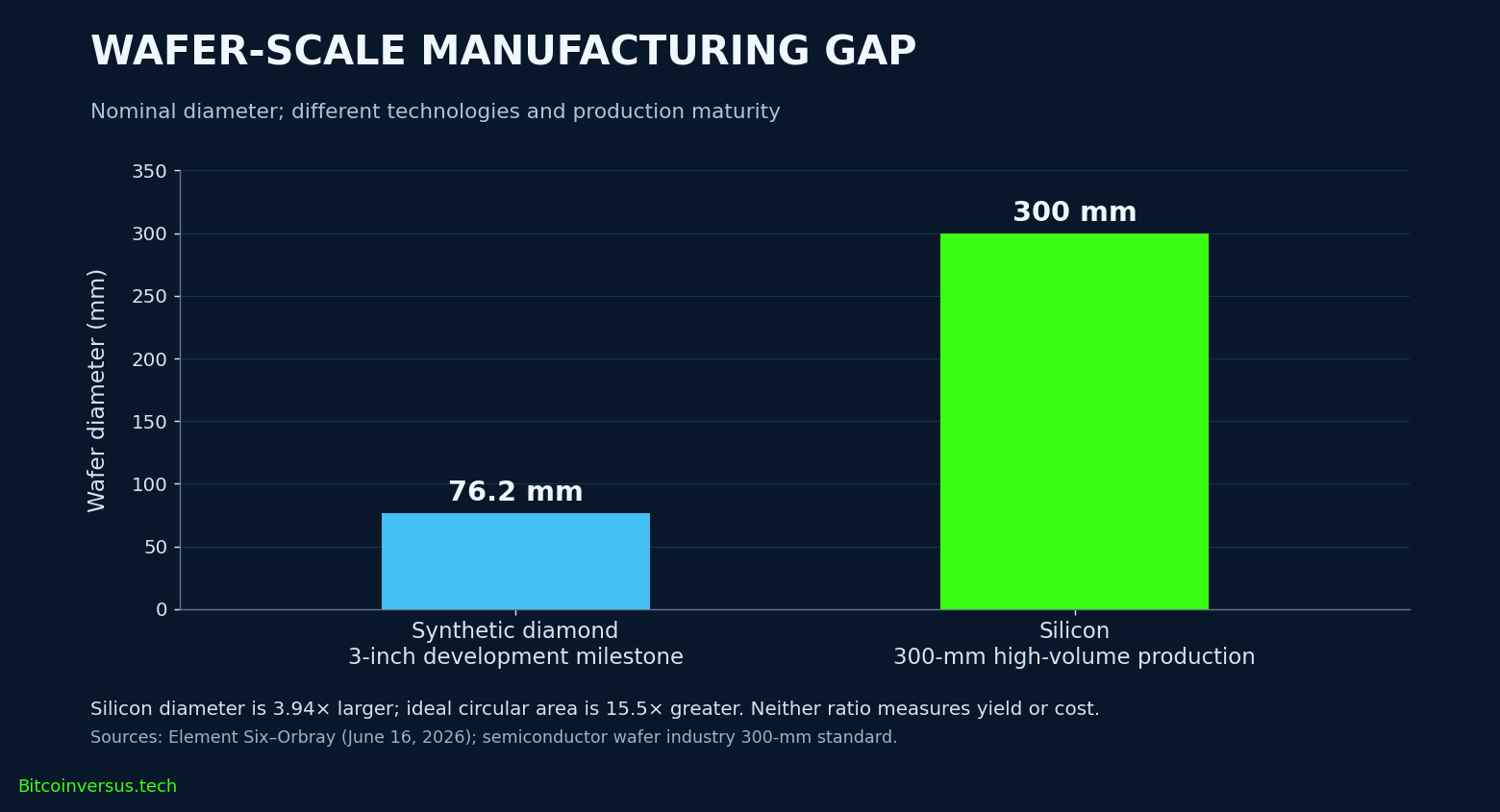
The size comparison is a manufacturing-readiness indicator, not a like-for-like price quotation. More area might support more devices, but actual yield depends on surface quality, edge losses, defects and compatible tools.
Is lab-grown diamond actually cheaper?
There is no verified public basis to declare the Entegris–Element Six diamond-integration route cheaper per finished semiconductor than established silicon-ingot wafer manufacturing. Entegris calls cost-effective wafer-level integration a development goal, not a measured commercial result. The companies have not disclosed a standardized cost per good package, defect yield, bonding throughput or diamond growth cost for the announced program.
A fair comparison must include diamond growth, slicing or shaping, surface finishing, bonding, thermal cycling, rejected devices and cooling-system savings. The engineering question is whether an added diamond layer produces enough value through reliability, heat removal or sustained computing performance to justify its extra package cost—not whether a diamond wafer can replace the silicon transistor substrate.
Element Six presents its copper–diamond composite for semiconductor thermal management in the company’s official video. Copper–diamond composite and pure CVD diamond are distinct material products; video source: Element Six.
Commercial proof will require system-level results
Prior BitcoinVersus.Tech coverage of Frore’s diamond-assisted design and Wiwynn’s diamond tests illustrates broader industry interest. Neither project establishes Entegris’s finished-device economics. Likewise, hybrid-bonding technology highlights why interface quality and manufacturing yield matter as much as bulk material performance.
Independent comparisons should report dollars per qualified package, watts removed at a defined junction temperature, defect rates and reliability under realistic operating cycles. Until suppliers publish comparable tests, synthetic diamond’s high conductivity is established; a production-cost advantage over silicon is not.
Primary sources and methodology
Element Six–Entegris partnership (November 3, 2026); Element Six thermal materials (accessed November 8); Element Six–Orbray wafer-scale announcement (June 16); NIST-hosted thermal conductivity reference; OSHA silicon substrate manufacturing guide; OECD semiconductor value-chain study (2025).
Editor’s Note: The thermal-conductivity figure compares bulk material properties near 300 K, not chip performance, and the supplier-grade interval is not an error bar. Wafer diameters describe separate manufacturing pathways; no market prices or production yields have been inferred. The 1200 × 630 cover is an original conceptual illustration, not a photograph of a deployed product. The Element Six video concerns copper–diamond composites, not confirmed Entegris prototype footage.
Support BitcoinVersus.Tech
To contribute an optional 5,000 satoshis, scan the original BitcoinVersus.Tech donation QR below with a compatible Bitcoin wallet. On a phone, display the article on another device or use a wallet’s supported saved-image scanning feature. Verify the payment destination and amount before sending.

We volunteer daily to ensure the information on this platform is Verifiably True. If you would like to support the research, please scan QR code.


Leave a Reply