
Researchers in Italy have demonstrated a tiny optical circuit that can generate, amplify and control light on the same chip at room temperature. The device uses caesium lead bromide perovskite rather than an ordinary silicon transistor architecture. The study, led by Antonio Fieramosca and Daniele Sanvitto at CNR Nanotec in Lecce, appeared in Nature on November 18, 2026.
The achievement targets a persistent problem in optical computing. Light moves quickly through waveguides, but manipulating one optical signal with another can require power-hungry materials, additional devices or extremely low temperatures. The team integrated several nonlinear optical functions using a crystal-growth process that also creates the microscopic structures guiding light.
Archival academic lecture by Prof. Michał Matuszewski, hosted on YouTube, discussing exciton-polaritons for integrated quantum and photonic technologies. Educational background, not a recording of the 2026 CNR experiment.
The chip uses particles that behave partly like light and partly like matter
The active material is CsPbBr3, a halide perovskite semiconductor. When light strongly couples to electronic excitations called excitons, the combined system forms exciton-polaritons. Their photon-like component helps them travel along a waveguide, while their matter-like component allows stronger interactions than ordinary photons have in many traditional optical materials.
To make the devices, researchers used a soft-lithography and microfluidic process to grow micrometre-wide crystal tracks with nanometre-scale gratings already formed along them. The gratings guide light into and out of the tracks and provide optical feedback. An example grating pitch measured 240 nanometres, according to the paper’s first figure.
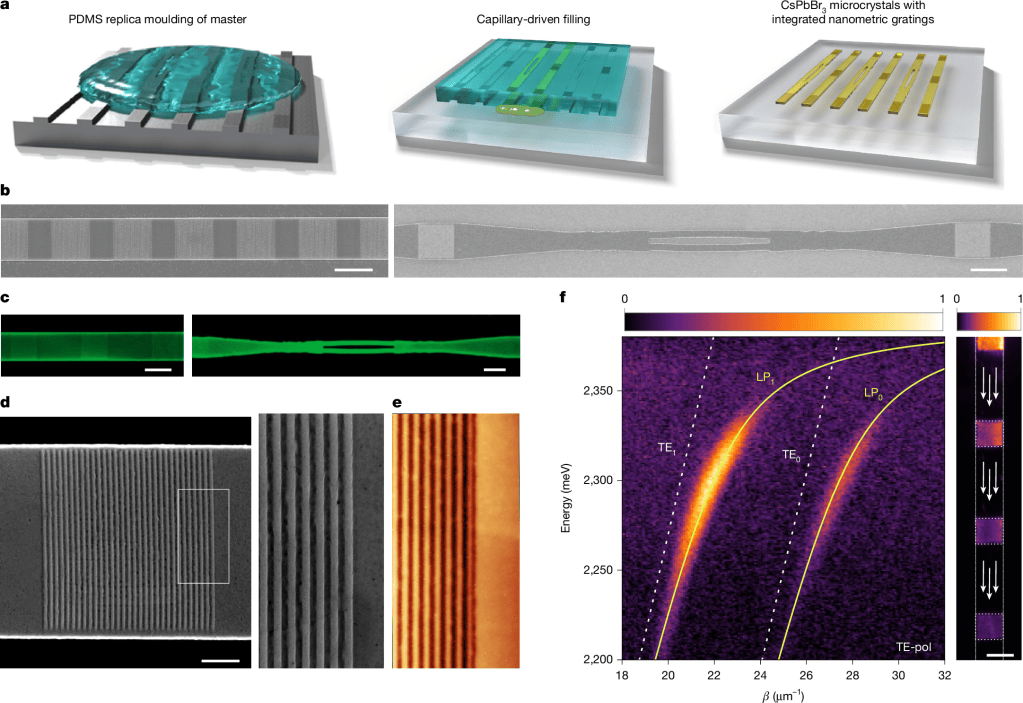
The results bring multiple operations onto the same type of structure: guided polariton lasing, amplification of an injected optical signal and controllable phase changes. The researchers report amplification approaching two orders of magnitude and phase shifts reaching 2π radians. Neither figure should be confused with a processor’s computing speed, efficiency or accuracy.
A laser, an amplifier and a controllable optical path
The miniature grating pairs form cavities that support coherent emitted light when excited above a threshold. By changing the grating geometry, the team altered the selected emission wavelength. An injected signal was also amplified by a separately excited region of the crystal. Optical phase control allowed an interferometer to convert phase changes into measurable output-intensity changes.
The design could eventually support compact optical switches or specialised analog and neuromorphic processors. The team does not demonstrate complete logic circuits, operating-system software or a data-centre accelerator. Earlier research covered by BitcoinVersus.Tech includes a 115-nanometre nanolaser for potential cell tracking and a 180 Gb/s optical transmitter; both address different components of the broader photonics problem.
Archival research lecture by Wei Bao about room-temperature perovskite polariton systems and their physical behaviour. The speaker describes related work, not the new CNR integrated circuit.
The remaining obstacle is electrical operation
Every reported function depended on external optical pumping, including laser excitation. Researchers still need electrically driven operation, stable device lifetimes, manufacturable interconnects and repeatable performance at useful scale. Perovskite materials may also raise durability and lead-containing material-handling questions.
Single-step crystal growth may reduce damage from later fabrication stages, but scaling from experimental structures to reliable chips requires testing yield, thermal behaviour and integration with electronics. Related advances in 81.92 Tb/s laboratory optical transmission and 25.9%-efficient perovskite solar cells illustrate different uses of light and perovskite crystals, not performance benchmarks for the CNR chip.
The confirmed result is a room-temperature experimental platform combining several optical functions in one material system. Whether it becomes a practical computing component will depend on measured power budgets, electrical pumping, reliability and reproducible device fabrication.
Research and source material
- Fieramosca et al., Fully integrated perovskite active polaritonic circuits, Nature, November 18, 2026, open access (CC BY 4.0)
- CNR Nanotec Advanced Photonics Laboratory: polaritonics research programme
- Nature Communications, 2024, previous perovskite active photonic device research
- Original authors’ December 2025 preprint, perovskite polaritonic circuits and nonlinear amplification
Editor’s Note: We volunteer daily to ensure the credibility of the information on our platform is Verifiably True. If you would like to support our work and the integrity of our research initiatives, scan the QR code below to donate 5,000 sats.

For mobile scanning, open the article on another display and scan the QR code with a Bitcoin wallet. Verify receiving address 3C9o19EH5HSiwEPyCTmEKzxhNCbo2X6TTb before sending.
BitcoinVersus.Tech publishes technology and engineering journalism for informational purposes and does not provide financial, investment, legal or professional engineering advice.


Leave a Reply