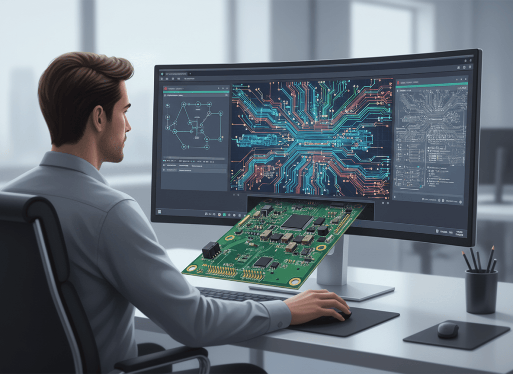
Printed circuit board design has traditionally required a fairly steep jump from an idea to a manufacturable design. A new company called heypcb is trying to compress that process by combining artificial intelligence with real electronic-design-automation files.
The platform allows a user to describe the machine or circuit board they want to build in ordinary language. HeyPCB then works toward creating the schematic, PCB layout and fabrication files inside a persistent project workspace. Unlike tools that only generate a picture or conceptual circuit diagram, HeyPCB says its service works with KiCad-native project files and can produce editable engineering outputs that can continue to be inspected outside the platform.
From Prompt to PCB
The basic idea is straightforward. A user can describe a device—such as a controller board, sensor system, robotics board or other embedded hardware—and allow the AI-assisted workflow to begin constructing the design.
HeyPCB says its system can work with verified component libraries, pin mappings and datasheet limits rather than placeholder parts. Its current product page says designs can be checked against real parts and fabrication rules before ordering, with electrical, layout and manufacturing checks applied to the actual board.
The workflow includes schematic creation, PCB layout, design-rule checking, imports and exports, autorouting and Gerber generation. HeyPCB’s terms of service also describe the product as an AI-assisted PCB design service that works with KiCad-native project files and may include DRC, autorouting, templates and Gerber exports.
KiCad Files Stay Portable
One of the more important parts of HeyPCB’s approach is file portability. The company says projects can be exported with Gerbers, STEP files and editable CAD, allowing the design to move into other tools or fabrication workflows instead of remaining trapped inside a proprietary format.
That matters because KiCad itself is built around real project files such as .kicad_sch for schematics and .kicad_pcb for board layouts. KiCad also includes a Gerber Viewer for reviewing fabrication output before a board is sent to manufacturing.
HeyPCB currently highlights open hardware reference projects including Pocket Science Lab, Watchy, Libre Solar BMS and OpenFC Lite Mini. These designs can be opened and inspected as starting points inside the platform.
Circuit World Adds a Hardware-Sharing Layer
HeyPCB is also building what it calls Circuit World, an online environment where designers can publish boards, inspect projects, fork designs and collaborate. The concept brings a software-development-style sharing model into PCB work, where a usable project has to include more than code: footprints, component selections, electrical constraints, dimensions and manufacturing data all matter.
The company is currently running a $1,000 Hardware Challenge through October 31, 2026. Participants design a board in HeyPCB, publish it to Circuit World and compete based on community likes. The announced prize package includes $500 cash, $500 in HeyPCB credit, an internship and an interview for a founding engineer role.
AI Does Not Eliminate Engineering Validation
HeyPCB also makes an important limitation clear: AI-generated designs can still contain errors. Its terms say automated outputs may be incomplete, incorrect, non-manufacturable or unsafe, and users remain responsible for reviewing and validating their designs before fabrication or deployment.
That is particularly important for power electronics, high-current systems, battery-management systems, RF hardware, medical equipment and other designs where an incorrect trace width, component rating, isolation distance or pin assignment can result in hardware failure.
BitcoinVersus.tech has previously examined the physical side of semiconductor development through Bitcoin ASIC Architecture: Bitmain, Canaan, MicroBT & Bitdeer and China’s CXMT Begins Mass Production of Fifth-Generation DRAM Platform. HeyPCB operates earlier in that hardware pipeline: the stage where an idea becomes a schematic, board layout and set of files that can eventually reach fabrication.
PCB Design Starts Looking More Like Software Development
HeyPCB represents a broader change across engineering software. Instead of manually creating every early design element, engineers may increasingly describe what they want, inspect the generated result, run automated engineering checks and then correct the remaining problems.
The important difference is that PCB design eventually has to leave the computer. A generated circuit must survive design-rule checks, electrical validation, manufacturing tolerances, assembly and real-world operation.
If HeyPCB can reliably connect conversational design with editable KiCad files and manufacturing-ready outputs, it could become part of a growing class of engineering platforms attempting to make hardware iteration move more like software development—without pretending that physical engineering constraints have disappeared.
BitcoinVersus.Tech Editor’s Note:
We volunteer daily to ensure the credibility of the information on this platform is Verifiably True. If you would like to support to help further secure the integrity of our research initiatives, please donate here: 3C9o19EH5HSiwEPyCTmEKzxhNCbo2X6TTb
https://x.com/1BitcoinVersus/status/1937006164555993338
BitcoinVersus.tech is not a financial advisor. This media platform reports on financial subjects purely for informational purposes.


Leave a Reply