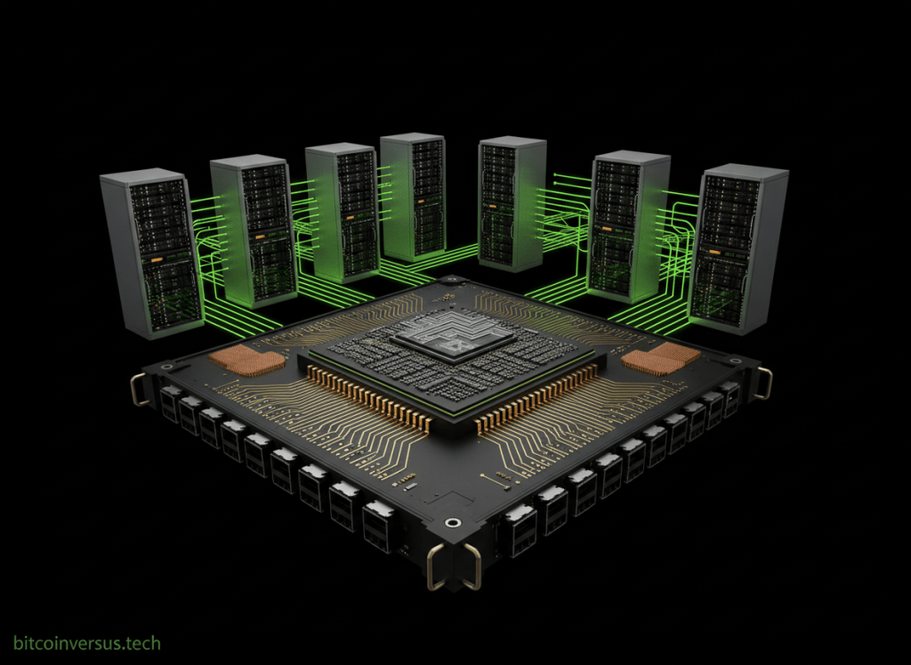
Marvell has taken its Teralynx T100 from an announced switch ASIC to a live public AI-networking demonstration. At AI Infra Summit 2026, the company showed the monolithic 3 nm Ethernet switch in both conventional BGA and co-packaged-copper configurations, pushing 102.4 Tbps of aggregate switching capacity into a single piece of switch silicon.
The September 16 demonstration gives the T100 a different significance from another paper launch. In a specific summit update, Marvell said the device was operating with a 512×200G radix and adaptive routing that responds to local queue depth, interface utilization and congestion information from remote switches.
Marvell’s summit announcement positioned the T100 as the Ethernet switching layer in a wider AI infrastructure portfolio spanning scale-up, scale-out and scale-across connectivity. The company also demonstrated PCIe switching, CXL memory systems, optical memory sharing and interconnect telemetry, but the T100 is the component that directly attacks the bandwidth and topology problem inside very large Ethernet fabrics.
102.4 Tbps on one switch die
The T100’s architectural headline is not simply that Ethernet reached another bandwidth tier. Marvell built the switch as a monolithic 3 nm device rather than combining multiple switching dies behind an internal fabric. That matters because every extra hop inside a multi-die switch can add latency, power and complexity before traffic even leaves the package.
The Next Platform’s technical analysis describes the chip as pushing close to practical reticle limits while integrating 512 working SerDes lanes. Marvell has cited 420-nanosecond port-to-port latency and typical power below 1,000 watts for the device, while offering package paths that include BGA, co-packaged copper and eventually optical integration.
The 512-port radix is especially consequential for AI clusters. Radix is the number of endpoints or network links a switch can directly expose. A higher radix can flatten a fabric by reducing the number of switching tiers required to connect a large accelerator population. Fewer tiers can mean fewer hops, fewer optical links and less accumulated latency between GPUs or other XPUs.
That progression fits the broader move BitcoinVersus.tech tracked as 1.6T Ethernet moved closer to data-center deployment. Faster individual links raise the bandwidth of each port; higher-radix switch silicon determines how many of those high-speed links can be concentrated into a useful fabric.
Adaptive routing watches congestion beyond one port
AI training traffic is unusually synchronized. Thousands of accelerators can finish one phase of work and then exchange large collective data sets at nearly the same time. A fabric with enormous headline bandwidth can still stall if too much traffic converges on the wrong paths.
Marvell says the T100’s adaptive routing uses more than the state of the immediately attached port. The switch can account for local queue depth, interface utilization and congestion metrics associated with remote switches, then steer traffic toward less-loaded paths. The objective is to keep more of the physical network usable when collective AI traffic becomes bursty.
This is where the switch ASIC and the optical layer meet. BitcoinVersus.tech recently covered Marvell’s 2 nm optical demonstrations for 3.2T AI networks. Those optical devices address how bits travel between packages and racks; T100 decides where Ethernet packets go once they reach the switching fabric.
Co-packaged copper attacks the shortest high-speed links
The summit demonstration also showed why packaging is becoming part of network architecture. In a conventional switch, very high-speed electrical signals must travel from the ASIC across the printed circuit board to front-panel connectors or pluggable modules. At rising SerDes rates, that electrical distance consumes signal margin and power.
Co-packaged copper moves the electrical interface closer to the switch package, shortening the highest-speed traces before the signal enters a cable. It does not replace optics for every distance. Instead, it gives designers another option for dense, short-reach links where copper can remain practical without forcing every connection into an optical module.
That packaging choice parallels the system-level shift described in BitcoinVersus.tech’s coverage of Micas expanding production of energy-saving AI network switches: AI networking is increasingly being optimized as a complete electrical, optical, thermal and switching system rather than as an isolated box with interchangeable ports.
The live demo moves T100 beyond the announcement stage
Marvell originally announced T100 earlier in 2026, so the September event should not be described as the chip’s launch. The fresh event is the hardware’s public demonstration. Marvell’s September 23 summit recap said the T100 made its first live public appearance since the original announcement and was the centerpiece of its booth.
A live demonstration still does not establish hyperscale deployment volume, independent benchmark leadership or field reliability. Marvell’s lowest-latency and lowest-power positioning remains a vendor claim unless tested under directly comparable conditions. What the summit does establish is that the 102.4 Tbps silicon exists beyond slides and was demonstrated publicly in two packaging configurations.
Ethernet is becoming specialized for AI
For decades, Ethernet’s advantage was that it was general-purpose and interoperable. AI is forcing Ethernet vendors to preserve that openness while adding behavior once associated with specialized high-performance fabrics: congestion awareness, extremely high radix, deterministic low latency and tighter integration between the switch package and its physical interconnect.
Teralynx T100 is a clear example of that transition. Its 102.4 Tbps capacity is the visible number, but the more important architectural story is how Marvell is combining a monolithic switch die, 512-port radix, adaptive routing and multiple package-level interconnect choices to make that bandwidth usable across large accelerator clusters.
BitcoinVersus.Tech
Advertisement
BitcoinVersus.Tech Editor’s Note:
We volunteer daily to ensure the credibility of the information on this platform is Verifiably True. If you would like to support to help further secure the integrity of our research initiatives, please donate here: 3C9o19EH5HSiwEPyCTmEKzxhNCbo2X6TTb
BitcoinVersus.tech is not a financial advisor. This media platform reports on financial subjects purely for informational purposes.


Leave a Reply