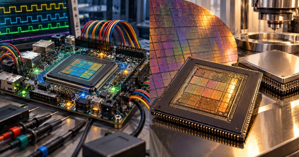
An FPGA and an ASIC can both turn an algorithm into hardware, but they solve opposite economic problems. An FPGA lets engineers reconfigure the hardware after manufacturing. An ASIC commits the hardware to a specific design before fabrication. That trade—flexibility versus specialization—changes performance, power, development cost, risk and time to market.
The short version is simple: choose FPGA when the design still needs to change; choose ASIC when the workload is stable enough and the production volume is large enough to justify permanent silicon.
| Category | FPGA | ASIC |
|---|---|---|
| Hardware | Reconfigurable after manufacturing | Fixed at fabrication |
| Time to first hardware | Usually faster | Usually slower |
| Up-front engineering cost | Lower | Much higher |
| Unit cost at large volume | Usually higher | Can become much lower |
| Performance per watt | Very good | Usually best for the target workload |
| Design changes after deployment | Yes | Generally no |
| Best fit | Prototypes, evolving standards, low/medium volume | Stable, high-volume, performance-critical workloads |
What an FPGA Actually Is
A field-programmable gate array is a chip containing configurable logic, memory, routing and often dedicated arithmetic blocks. Engineers do not merely load software onto an FPGA in the normal CPU sense. They configure the chip so its internal logic and interconnect implement a digital circuit.
AMD’s FPGA architecture documentation describes logic elements and routing controlled by configuration memory, with structures such as configurable logic blocks, I/O, clocking, block RAM and DSP resources. A lookup table can implement Boolean logic, while flip-flops store state and programmable routing connects the pieces into a custom datapath.
That flexibility is the FPGA’s superpower. A design can be synthesized, placed, routed and loaded as a new bitstream without fabricating another chip. Our earlier FPGA explainer walks through that architecture in more detail.
What an ASIC Actually Is
An application-specific integrated circuit takes customization further. Instead of mapping a design onto a prefabricated grid of programmable logic, engineers create circuitry for the intended function and manufacture that circuitry into silicon. Synopsys’ ASIC design overview describes the process as developing an integrated circuit optimized for a predefined application, from architecture through physical layout and manufacturing.
That removes much of the overhead required to make an FPGA reconfigurable. An ASIC does not need a sea of generic lookup tables and programmable routing for logic that will never change. Transistors, wires, memories and arithmetic units can instead be optimized around the final workload. The result can be higher clock efficiency, greater density, lower latency and better performance per watt.
They Often Start With the Same RTL
The two paths can begin surprisingly close together. Engineers commonly describe digital hardware in Verilog, SystemVerilog or VHDL. Simulation and verification test whether the register-transfer-level design behaves correctly. Synthesis then converts that RTL into logic.
From there the flows diverge. For an FPGA, implementation maps the logic into the exact LUTs, registers, DSP blocks, RAM and routing resources available on the selected device. Place-and-route tools produce a configuration bitstream that can be loaded onto hardware.
For an ASIC, synthesis is only the beginning. The design must move through floorplanning, placement, clock-tree work, routing, timing closure, power analysis, design-for-test, physical verification and signoff before tape-out. Masks are then created and wafers fabricated. An FPGA compile can be repeated; an ASIC error discovered after fabrication can require an expensive new silicon revision.
Why ASICs Usually Win on Performance and Power
Programmability costs silicon. FPGA routing needs configuration switches, programmable logic needs extra transistors, and general-purpose resources are not always the perfect shape for a specific function. Those features are valuable because they let the hardware change, but they consume area and power.
An ASIC can eliminate that flexibility tax. A fixed datapath can place exactly the required arithmetic near exactly the required memory and interconnect. That is why ASICs dominate workloads where the algorithm is stable, efficiency matters enormously and enough units will ship to recover development cost.
Why FPGAs Still Matter
Raw efficiency is not the only engineering metric. An FPGA can reach the lab or field long before a custom chip returns from fabrication. Bugs can be corrected with a new bitstream. Interfaces can be changed. Algorithms can evolve. Companies can build specialized hardware without paying for a complete custom-silicon program.
This makes FPGAs especially valuable for prototyping ASICs, industrial control, test equipment, networking, aerospace, software-defined radio and products built around changing standards. Embedded FPGA blocks can even put reconfigurable logic inside an SoC; our report on QuickLogic’s eFPGA design shows how that middle ground is expanding.
The Cost Curve Is the Real Battle
An FPGA has a relatively low barrier to entry because the silicon already exists. Engineers buy the device, build the design and program it. But every production unit still contains all of the circuitry that makes the FPGA programmable.
An ASIC reverses that cost structure. Non-recurring engineering can include architecture, verification, EDA tools, physical design, IP, masks, packaging and fabrication. That can make the first working chips extraordinarily expensive. Once the design is mature and production volume becomes large, however, the per-unit economics can favor the ASIC because the finished die contains only what the product requires.
There is no universal break-even quantity. Process node, die size, package, mask set, engineering team, FPGA price, yield and expected lifetime all change the calculation. The correct question is not “How many units make ASIC cheaper?” but “Will the lifetime savings in unit cost, power and performance repay the non-recurring engineering and schedule risk?”
Bitcoin Mining Shows the Transition Perfectly
Bitcoin mining is one of the cleanest demonstrations of the FPGA-to-ASIC transition. Early miners used CPUs and then GPUs. FPGAs followed because SHA-256 could be implemented as dedicated hardware pipelines while retaining reprogrammability. But Bitcoin’s proof-of-work algorithm was stable and the economic reward for better hashes per joule was enormous.
That made the ASIC investment rational. Once companies could justify custom silicon, fixed-function SHA-256 chips displaced FPGAs because mining rewarded exactly what ASICs do best: execute one stable computation repeatedly, at enormous scale, using as little energy and silicon as possible. Our history of Bitcoin mining’s CPU-to-ASIC evolution traces that progression.
Which One Should You Choose?
- Choose FPGA when requirements can change, volumes are uncertain, time to market matters, hardware must be field-upgradable, or the ASIC business case is not yet proven.
- Choose ASIC when the workload is stable, the product will ship at sufficient scale, power and performance matter enough to justify custom silicon, and the organization can absorb the cost and risk of tape-out.
- Use both when an FPGA is the prototype and validation platform for a later ASIC, or when a system combines fixed-function silicon with a smaller region of reconfigurable logic.
Bottom Line
An FPGA is custom hardware you can change. An ASIC is custom hardware you manufacture. The FPGA buys flexibility with extra silicon and power overhead; the ASIC buys efficiency by locking the design down. Neither is automatically better. The right answer depends on whether the economic value of specialization exceeds the cost of giving up reconfigurability.
BitcoinVersus.Tech Editor’s Note:
We volunteer daily to ensure the credibility of the information on this platform is Verifiably True. If you would like to support to help further secure the integrity of our research initiatives, please donate using the QR code provided

For best QR-code scanning results, please scan this donation code from a desktop or larger screen. Mobile screens may prevent camera recognition.


Leave a Reply