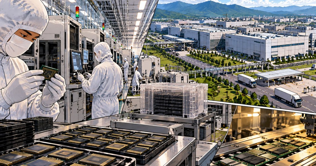
A fresh r/Economics thread pushed Samsung’s semiconductor expansion back into view, but the important detail is what is actually being built: a large back-end memory testing operation in northern Vietnam, not a new leading-edge wafer fab.
According to documents reported by Seoul Economic Daily, Samsung Electronics plans two memory test fabs at Yen Binh Industrial Park in Thai Nguyen. The reported investment totals about 105.79 trillion Vietnamese dong, or roughly $4.09 billion. The facilities are intended to perform final testing on DRAM and NAND packaged in Cheonan, South Korea, with the first line targeted for the fourth quarter of 2027 and additional capacity planned for 2028.
The move fits the larger AI-memory buildout already affecting DRAM supply and Samsung’s push to increase HBM4 output. Moving more conventional back-end testing abroad can free Korean capacity for higher-value memory and packaging work.
Samsung Electro-Mechanics is making a separate 6.78 trillion won FCBGA investment across Sejong and Vietnam. The company says demand for larger, higher-layer-count substrates is being driven by AI servers. That is the same advanced-packaging pressure seen across the wider AI chip supply chain.
The key distinction is simple: Vietnam is becoming more important in Samsung’s testing and packaging chain, while the highest-value memory production remains centered in South Korea. That split shows how AI demand is reshaping not only chip fabrication, but every step after the wafer leaves the fab.
BitcoinVersus.Tech Editor’s Note:
We volunteer daily to ensure the credibility of the information on this platform is Verifiably True. If you would like to support to help further secure the integrity of our research initiatives, please donate using the QR code provided

For best QR-code scanning results, please scan this donation code from a desktop or larger screen. Mobile screens may prevent camera recognition.


Leave a Reply