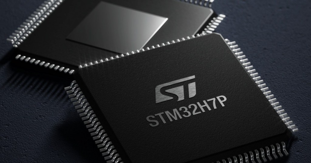
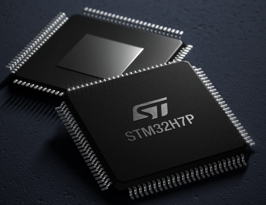
STMicroelectronics introduced the STM32H7P industrial microcontroller family on November 4, 2026, combining a 520 MHz Arm Cortex-M7 processor with a dedicated neural accelerator and hardware signal processor. The chips target motor drives, solar inverter protection, industrial sensing and other embedded controls that must respond predictably while processing more complex signals.
The integrated Neural-ART accelerator is rated at up to 85 billion operations per second (GOPS), while the CPU achieves 2,773 CoreMark in ST’s disclosed configuration. OEM sampling is underway, but volume production is planned for January 2027. Neither the rated accelerator throughput nor the internal benchmark results prove performance in every industrial design.
Neural inference and signal processing share the workload
An industrial microcontroller repeatedly reads sensors, runs control algorithms and updates outputs within strict timing budgets. Running neural-network inference entirely on its main CPU can compete with control loops for processing time and memory access. STM32H7P instead pairs the Cortex-M7 with ST’s Neural-ART neural-processing unit and Hardware Signal Processor (HSP) for selected signal-processing operations such as transforms and vector calculations.
ST reports that its solar arc-fault detection model runs up to 40 times faster on the NPU than in its CPU software comparison. Separate company tests claim 20-fold acceleration for an anomaly detector and 15-fold for a battery-management model. Those figures describe different workloads and software configurations; they are not independent third-party measurements, energy savings or guarantees of equivalent acceleration in deployed products.
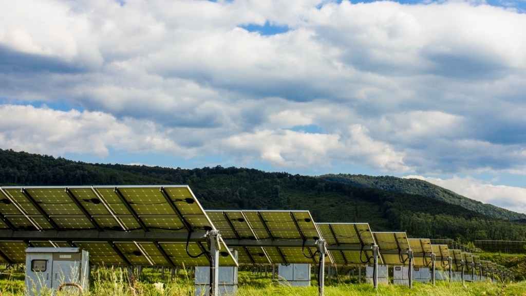
Solar arc-fault interrupters look for electrical signatures that can indicate dangerous arcing in photovoltaic circuits. Faster model execution could increase the time budget available to monitor multiple channels, but safety certification depends on false-positive rates, fault coverage, response time and system-level validation—not inference throughput alone. Related BitcoinVersus.Tech reporting covers ST’s different STM32G5 digital-power MCU and Renesas’ industrial motor-control processor.
Memory architecture favors real-time operation
The STM32H7P family offers up to 2 MB of dual-bank flash and 736 KB of RAM, including up to 320 KB of tightly coupled memory. The latter provides predictable, low-latency access for time-critical code and data, while 320 KB of AXI-connected RAM supports wider data movement. Engineers still have to schedule competing accelerator, CPU and direct-memory-access transfers to prevent jitter and bus contention.
ST lists four 12-bit analog-to-digital converters, two high-resolution timers, three motor-control timers and multiple CAN-FD interfaces. The chip does not integrate Ethernet, a graphics processor or display controller. Designers needing those functions must add external hardware or choose a different controller, affecting bill of materials, board space and firmware complexity.
Pricing, heat and testing still matter
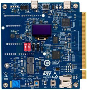
ST lists pricing from $4.43 per chip for a 1 MB flash device in an LQFP100 package at a 10,000-unit order quantity. The NUCLEO-H7P5II evaluation board and STM32H7P5IDK Discovery kit are scheduled for January 2027. ST says the family supports industrial ambient temperatures up to 125°C, but its detailed engineering note associates a 125°C full-load example with 350 MHz, not the maximum 520 MHz clock.
ST’s device listing currently identifies limited engineering samples under characterization. Independent thermal validation, motor-control stress tests, fault injection and hardware-in-the-loop testing remain necessary before safety-sensitive deployments. BitcoinVersus.Tech’s earlier guide to brownout reset diagnostics highlights an additional reliability issue a neural accelerator cannot eliminate.
The decisive next evidence will come from production silicon, published application-level power measurements, independent validation and customer qualification in 2027. Until then, the STM32H7P represents an announced architecture and early sampling program rather than proven mass-market industrial deployment.
Editor’s Note: Primary evidence comes from STMicroelectronics’ November 4 announcement, its November 3 engineering explanation and the manufacturer’s device specifications. Independent industry coverage from EE Times and IN Electronics & Design provided cross-checks. AI inference speedups are ST-reported results rather than independent field observations. Three images are sourced from official ST material; no YouTube player is represented as tested.
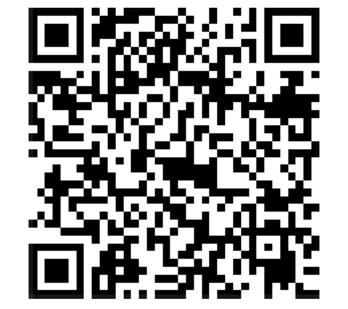
To donate 5,000 sats, open the article on a second screen and scan the original QR code using a compatible Bitcoin wallet. Mobile wallets supporting QR image import may scan a saved image. Verify the destination 3C9o19EH5HSiwEPyCTmEKzxhNCbo2X6TTb before sending.
We volunteer daily to ensure the information on this platform is Verifiably True. If you would like to support the research, please scan QR code.
BitcoinVersus.Tech publishes technical and financial coverage for educational purposes only. It does not provide investment advice.


Leave a Reply