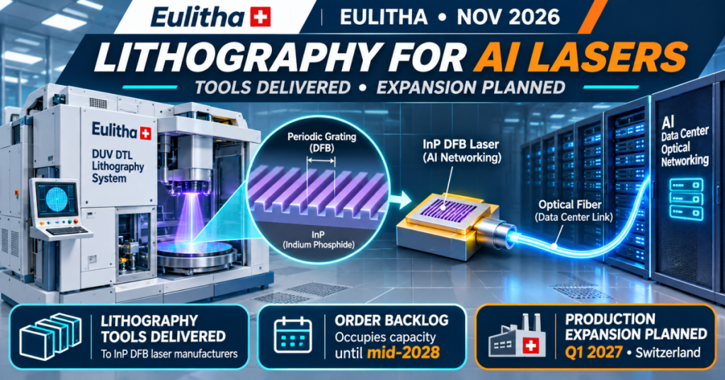
Swiss semiconductor-equipment company Eulitha has delivered multiple automated deep-ultraviolet lithography tools to foundries making indium-phosphide distributed-feedback (DFB) lasers for AI data-center communications. A company announcement posted November 4, 2026, carrying a November 2 dateline, also disclosed an order backlog sufficient to occupy existing tool-production capacity until the middle of 2028. Eulitha did not disclose the number of newly delivered systems, individual customers, order values or the volume of lasers produced.
Modern AI clusters move enormous volumes of information between processors, switches and memory systems. Optical transceivers translate electrical signals into light for fiber links, helping transport data between equipment racks and across longer distances. DFB semiconductor lasers use precisely patterned optical gratings to select a narrow wavelength, making grating uniformity a manufacturing concern rather than a cosmetic detail.
Printing nanometer-scale gratings for AI lasers
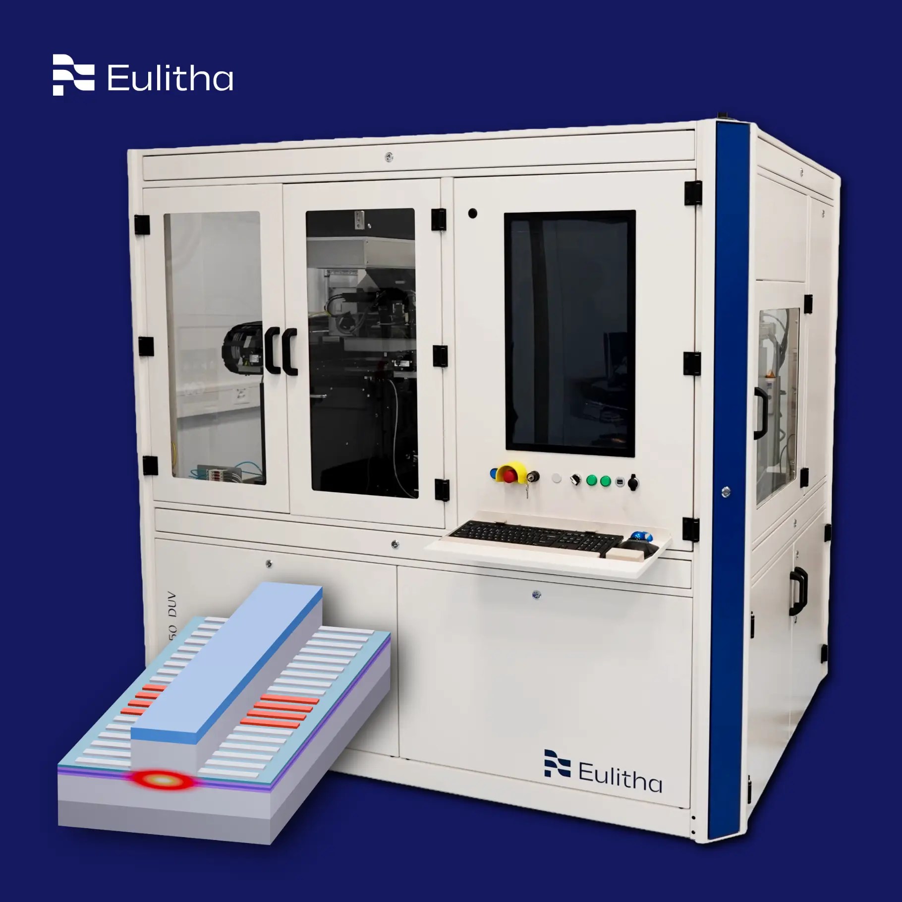
The company’s proprietary Displacement Talbot Lithography (DTL) process illuminates a periodic mask and uses the resulting diffraction-interference field to expose photoresist while the substrate moves through the pattern. The approach prints repeating nanoscale structures without direct mask contact. Eulitha says its process reaches approximately 60-nanometer feature dimensions and offers a comparatively large effective depth of focus, useful for surfaces that are not perfectly flat.
Photolithography creates patterns in light-sensitive materials before subsequent processing transfers them into functional structures. BitcoinVersus.Tech previously explained how photoresist patterning works and why overlay accuracy matters. DTL is optimized for periodic structures; it should not be confused with the full range of projection lithography tools used to fabricate leading-edge logic transistors.
The company’s DFB laser technical flyer describes photonic grating pitches down to 120 nanometers for one product line, plus chirped and phase-shifted designs. Such specifications describe the tool’s patterning capability, not measured output yield at the recently supplied foundries.
Delivered equipment versus future capacity
Eulitha says manufacturers have already used its lithography platforms for DFB laser production over several years, and the new announcement covers additional delivered tools. Separately, the company is doubling its own equipment-manufacturing capacity near Zurich, with the expansion scheduled to begin operating in the first quarter of 2027. Neither the planned expansion nor the order backlog is equivalent to laser-production capacity already available at customer fabs.
The mid-2028 backlog suggests sustained customer interest, but Eulitha provided no financial valuation, backlog conversion schedule, or independent order audit. Its chief executive argues that optical lithography can be more economical than deploying numerous electron-beam writing tools for repeating patterns. Actual savings will vary with mask costs, throughput, process yield and fab integration.
Optics must still pass system-level tests
An optical transmitter still needs suitable modulation electronics, packaging, thermal stabilization and qualification before installation. BitcoinVersus.Tech has covered Tower and Innolight’s near-package optical chips and photonics manufacturing specifications for AI facilities. Readers can also consult the guide to optical transceivers for the distinction between laser sources, transceiver modules and complete data-center links.
More laser-patterning equipment could relieve one production bottleneck as AI clusters expand. However, the company has not demonstrated that its newly delivered tools increased industrywide transceiver shipments, reduced energy use at a customer site, or solved other optical supply-chain constraints. The near-term milestones are customer qualification, output yield and the planned Swiss capacity expansion—not an already completed transformation of data-center networking.
Primary sources: Eulitha’s November 2026 deliveries announcement; DTL technology explanation; official equipment portfolio; and DFB lithography technical flyer.
Editor’s Note: Eulitha’s release appears with a November 4, 2026 posting date and November 2 dateline. The company confirms multiple equipment deliveries but does not identify the number of machines, customers or laser production output. Its mid-2028 backlog and first-quarter 2027 production expansion are company statements and plans, not independently audited future results. The featured cover and technical diagrams are conceptual artwork; the PhableX image is an official manufacturer photograph.
Support BitcoinVersus.Tech
Support independent reporting by scanning the original approved QR code below for an optional 5,000-satoshi donation. Mobile readers can open the article on another screen to scan using a compatible Bitcoin wallet, or use a wallet’s image-scanning function if supported. Verify the receiving address and amount before sending funds.

We volunteer daily to ensure the information on this platform is Verifiably True. If you would like to support the research, please scan QR code.


Leave a Reply