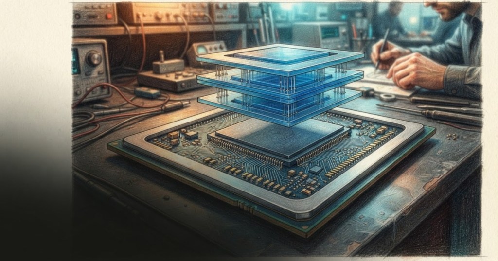
Preferred Networks and SEMIFIVE announced a new application-specific AI processor collaboration on November 16, 2026, with Samsung Foundry providing manufacturing technology for the logic chip. The planned MN-Core L2000 Series will stack dynamic random access memory, or DRAM, above processor logic. Its principal target is more than twice the memory bandwidth of Preferred Networks’ earlier L1000 design, which itself is not scheduled for release until 2027.
The companies plan to complete the L2000 design and send it to the foundry, a milestone called tape-out, during the first quarter of 2027. No commercial shipment date or independently tested inference benchmark has been announced. The L2000 remains a development project, not a shipping competitor to existing GPU clusters.

Why memory bandwidth drives the design
AI inference converts a trained model into outputs such as text, images or decisions. Large models repeatedly retrieve weights and intermediate data from memory, so arithmetic units may sit idle when memory cannot feed them quickly enough. Increasing peak operations per second alone does not remove that bottleneck. Preferred Networks says its L series aims to move data more efficiently by shortening the paths between memory and computation.
Conventional AI servers often use packages with high bandwidth memory, or HBM, beside the processor. A vertically integrated design places DRAM above the logic, creating many short electrical paths across the stack. The layout can increase bandwidth density, but practical gains depend on interconnect signaling, memory capacity, usable bandwidth, workload size and thermal design. Our earlier explainer on HBM architecture provides background on established alternatives.
Archival MN-Core overview video embedded on Preferred Networks’ official chip technology page. It explains the company’s processor family; it is not a demonstration of working L2000 production hardware.
Three companies, three engineering roles
Preferred Networks leads the processor architecture and logical design. SEMIFIVE handles implementation, advanced packaging coordination and semiconductor supply-chain management. Samsung Foundry supplies the logic manufacturing platform and 3D integration design infrastructure, including connections between stacked dies and power delivery methods. The Elec reports that the platform also targets fewer packaging components and an alternative path around HBM supply constraints.
The combination creates engineering challenges. Higher heat density can make an otherwise fast stack difficult to cool; vertical connections complicate manufacturing yield, inspection and power integrity. Preferred Networks’ leadership explicitly acknowledged thermal management, power consumption and yield as development risks. The partners have not provided L2000 power draw, physical dimensions, core count, memory capacity, foundry process node or price.
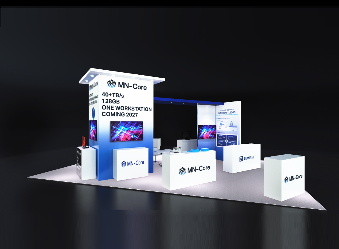
What 2× actually measures
The headline compares a target bandwidth for the future L2000 with a target for the unreleased L1000. It is not evidence of twice the token generation speed, twice the application throughput or twice the efficiency of a commercially available NVIDIA product. Those metrics require comparable workloads, precision formats, batching and measurements taken on finished systems.
Preferred Networks first described the L1000 in November 2024, planning stacked DRAM and dedicated arithmetic hardware. Its existing MN-Core family has a history of energy-efficient supercomputing, but earlier results cannot be transferred automatically to the new series. The company intends to show its L series roadmap during the SC26 supercomputing conference in Chicago, November 17 to 19.
Other chip developers are pursuing similar memory strategies. BitcoinVersus.tech reported Fractile’s stacked memory inference project; our coverage of SEMIFIVE and Mobilint’s robotics chip concerns a separate customer and architecture. Samsung’s foundry expansion plans also provide industry context, without establishing a process node for L2000.
The next milestone is silicon
Successful tape-out would mark completion of design work for manufacturing, not proven mass production. Fabricated samples, package reliability, cooling requirements and comparable inference benchmarks must follow before operators can evaluate deployments. More bandwidth could help reduce inference delays and power usage, but the announcement remains a roadmap milestone until production silicon demonstrates measurable advantages.
Original sources: Preferred Networks and SEMIFIVE announcement, November 16, 2026; Preferred Networks’ SC26 exhibition notice; L1000 original architecture announcement.


Leave a Reply