
British AI-chip developer Fractile raised $720 million in a Series C financing announced November 11, 2026, at a $7 billion post-money valuation confirmed by participating investor Balderton. Thrive Capital, Founders Fund, Lightspeed and Redpoint co-led the round. UK government investment came through Sovereign AI and the British Business Bank, with individual state contributions undisclosed. Fractile wants to speed large AI models by stacking memory directly over compute logic, but its first chips and systems remain scheduled for 2027, not commercial deployment today.
No Priors, “Frontier Chips for Frontier AI Labs,” October 2, 2026. Fractile founder Walter Goodwin discusses memory bottlenecks, chip design and model inference with Sarah Guo. Recorded before the November financing; not a demonstration of a shipping Fractile processor. Credit: No Priors / YouTube.

Why memory location determines AI response speed
Inference is the process of generating output from an already-trained model. During token generation, processors repeatedly retrieve model weights and attention data, including the key-value cache for earlier context. When arithmetic units wait for memory, adding theoretical compute capacity alone cannot eliminate latency. Earlier BitcoinVersus.Tech coverage explains high-bandwidth memory and the capacity-versus-latency trade-offs of SRAM and DRAM.
Modern GPU packages commonly place vertically stacked HBM devices beside a logic die, connected through advanced packaging. Fractile instead proposes placing custom DRAM directly over processing logic. Shorter, wider connections could increase effective memory access bandwidth while retaining more capacity than on-chip SRAM. Investors describe a major potential bandwidth gain, but they have not supplied independently reproducible production-chip measurements establishing its magnitude.
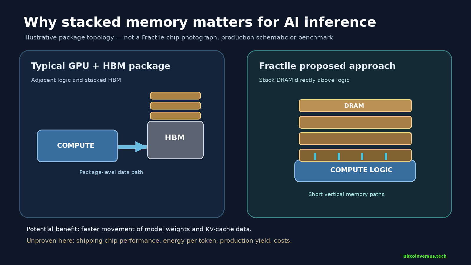
Physical integration creates other engineering constraints. Closely packed memory and logic can complicate heat removal, die-to-die signaling, packaging yield, test access and repair economics. Bandwidth alone cannot establish tokens per second, watt-hours per million tokens or total cost of ownership. Those comparisons require equivalent model sizes, context lengths, batch sizes, cooling conditions and software stacks.
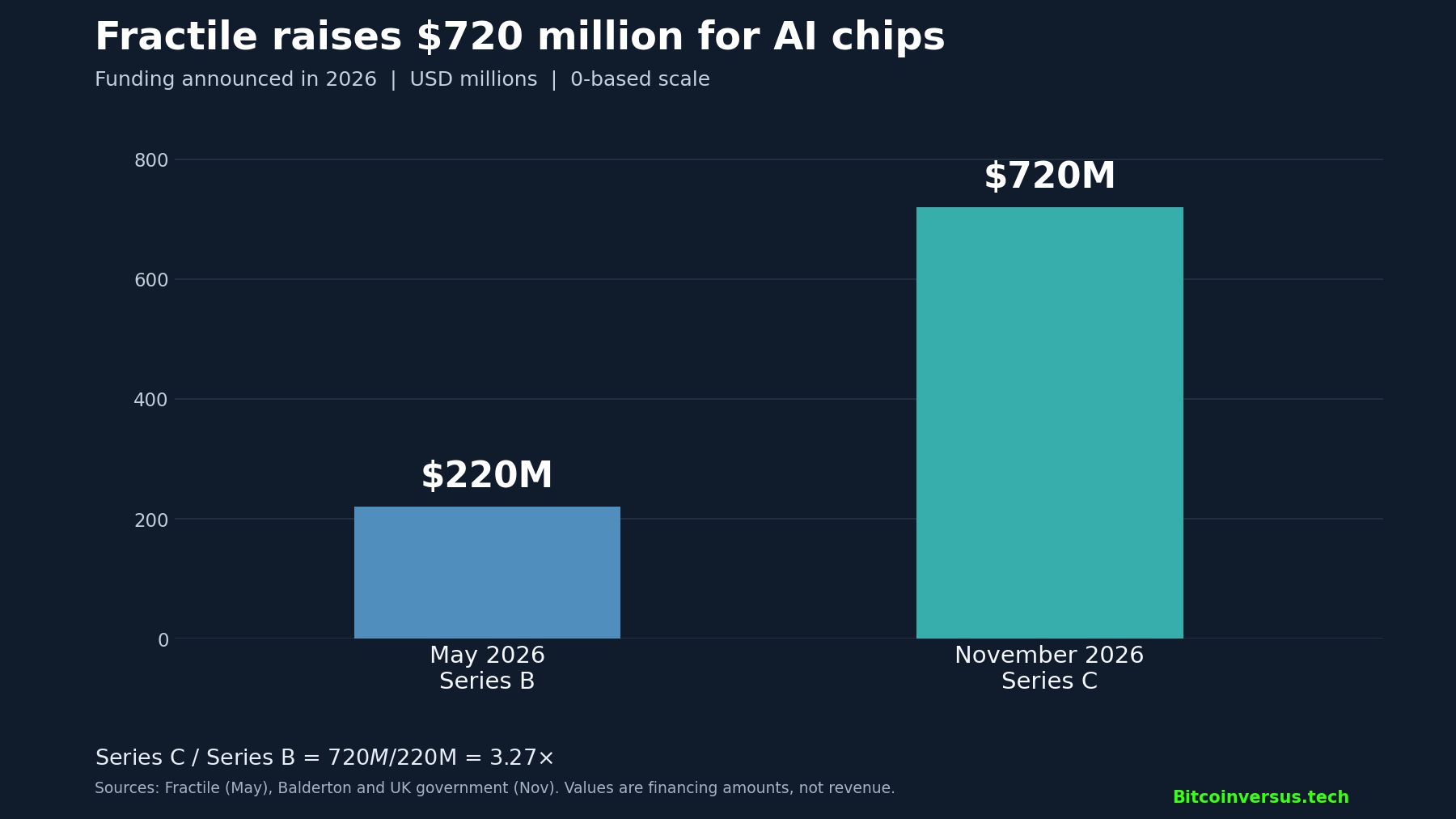
The new round is 3.27 times May’s funding
Fractile disclosed a $220 million Series B in May. The new $720 million round is $500 million larger, or 3.27 times the prior financing amount: $720 million ÷ $220 million = 3.27. Its $7 billion post-money valuation is an investor transaction price, not revenue, an audited asset value or evidence that a chip has met commercial specifications. The UK government’s announcement described a financing exceeding £500 million but did not identify how much the state itself invested.
A 2027 shipment target still requires independent tests
Chief executive Walter Goodwin says the funding should support the first chips and systems shipping in 2027. He has discussed much higher memory-access speeds, while investment partners promote faster inference at lower cost. None of those claims represents a standardized benchmark on a broadly available Fractile production system. The company has not publicly established independently tested chip yields, sustained production throughput, per-token energy savings or a fleet-wide commercial deployment count.
Competition extends beyond NVIDIA GPUs. d-Matrix’s 1,024-chip inference cluster and its NVLink Fusion integration strategy represent different accelerator and networking approaches. Memory supply matters as well: HBM demand has affected ordinary DRAM pricing, raising questions about manufacturing capacity and component costs for new entrants.
Fractile’s end-to-end software and compiler plans may prove as important as its physical package. A chip with attractive peak bandwidth can still lose performance through memory fragmentation, scheduling, networking or weak software support. Broader coverage of next-generation chatbot accelerators explains why latency must be evaluated at the application level. Fractile has raised substantial capital to test a credible engineering hypothesis; the decisive milestones remain delivered silicon, reproducible model benchmarks and customers operating it at scale.
Sources and calculations: Balderton announcement, November 11, 2026; UK government investment announcement, November 11; Fractile founder’s May 13 Series B announcement; Lightspeed technical investment analysis; Reuters report via Euronext, November 11; TechCrunch independent coverage, November 11; No Priors interview, October 2. Calculation: $720M ÷ $220M = 3.27×; $720M − $220M = $500M. Funding figures and claimed technical advantages are distinct from audited product revenue and measured chip benchmarks.
Editor’s Note: Fractile’s November 2026 $720 million financing and $7 billion post-money valuation are supported by investors and independent reporting. UK government participation is confirmed, but its individual contribution was not disclosed. Fractile’s DRAM-on-logic architecture and proposed speed advantages remain company- and investor-described; an independently benchmarked shipping processor was not identified. First-chip shipments in 2027 are targets, not completed deliveries. The featured cover and architecture diagram are original conceptual illustrations, not product photographs or verified schematics. The original funding chart uses a zero baseline and clearly distinguishes financing from revenue. The official Fractile founder photograph predates the financing. The October No Priors interview supplies background, not proof of hardware performance. WordPress’s rendered output confirms a YouTube iframe with the intended No Priors video ID; actual playback, physical mobile-device layout and live-browser display were not verified.

BitcoinVersus.Tech is volunteer-run and publishes independent educational technology reporting. An optional 5,000-satoshi donation helps support continued research. Scan the original QR from a second screen using a compatible Bitcoin wallet; on mobile, use a wallet that can scan a QR saved as an image. Independently verify the recipient address 3C9o19EH5HSiwEPyCTmEKzxhNCbo2X6TTb and amount before sending. Bitcoin transactions are generally irreversible.
We volunteer daily to ensure information on the BitcoinVersus.Tech platform is Verifiably True. Coverage is for educational and informational purposes and does not constitute financial or investment advice.


Leave a Reply