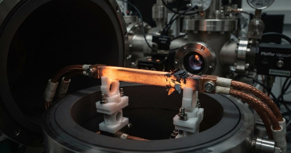
Scientists at South Korea’s Institute for Basic Science have turned electromigration, a mechanism that can damage electronic circuits, into a way to grow graphite at chosen locations. The team drove carbon through heated nickel and cobalt using direct electrical current, forming graphite as far as 8 to 10 millimeters from the original carbon source. Its results appeared in Advanced Materials on October 28, 2026, followed by an Institute for Basic Science announcement on November 19.
Official UNIST interview with Rodney Ruoff, director of the research center, published April 2026. The archival video introduces the team’s carbon-materials research; it does not show the October paper’s experiment.
A circuit failure mechanism becomes a fabrication tool
In ordinary integrated circuits, sustained current can move atoms along tiny metal interconnects. The resulting voids and accumulations may raise resistance or break a connection. The new study tests a different application: directional transport of dissolved carbon atoms through a solid metal lattice at high temperature.
Researchers placed carbon at the center of nickel and cobalt bars and heated the assemblies symmetrically. After 50 hours under direct current, carbon accumulated toward the negative electrode, known as the cathode, and precipitated into graphite. Under comparable heating with alternating current, which reverses direction repeatedly, researchers observed only thin deposits close to the initial source.
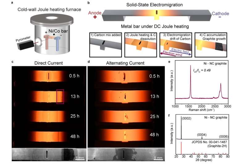
The thickest graphite layers under direct current were approximately 300 to 450 times thicker than those produced under the alternating-current control. The multiplier compares layer thickness under the researchers’ laboratory conditions, not manufacturing speed or overall graphite output. Comparable heating between tests helps isolate the influence of current direction.
Electric current also selects between carbon isotopes
A second finding involves carbon-12 and carbon-13, two stable isotopes that differ by one neutron. Raman and mass-spectrometry measurements showed that graphite deposited at the collection site was enriched in the lighter carbon-12 isotope. One nickel experiment began with 47.4% carbon-13 and recovered graphite with 38.4% carbon-13, a decrease of 9.0 percentage points.
Across multiple source compositions, researchers measured a carbon-12 to carbon-13 ratio in recovered graphite approximately 29% to 62% higher than in the starting material. Their atomic simulations predicted carbon-12 hopping about 4% faster than carbon-13, but simulations underestimated enrichment in some isotope-rich samples. The mechanism is promising, not completely settled.
ChipCraft’s December 2024 semiconductor reliability presentation covers conventional electromigration damage beginning around 26:50. Archival educational context; not a recording of the IBS graphite-growth experiment.
Why graphite’s thermal performance matters
Graphite can carry heat efficiently along its stacked carbon layers. Using frequency-domain thermoreflectance, the team reported approximately 2,003 watts per meter-kelvin of in-plane thermal conductivity for graphite made from naturally abundant carbon. A sample with intermediate isotope composition measured approximately 1,750 W/m·K. The decrease is (2,003 − 1,750) ÷ 2,003 × 100, or 12.6%.
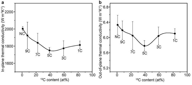
Those data show a relationship between isotope composition and heat transport, but do not prove a ready-made cooler for processors. Earlier BitcoinVersus.Tech reports examine diamond materials proposed for AI-chip cooling, the thermal trade-offs between diamond and silicon, and the broader graphene and photonics materials outlook. Different materials, geometries and operating temperatures cannot be compared through a single conductivity number.
An experiment, not a graphite factory
The study required sustained elevated temperatures, carefully prepared metal bars and roughly two days of current flow. The team has not demonstrated inexpensive, industrial-scale output or production in operational computer interconnects. Nor should the graphite be confused with commercial battery anodes, whose cycling and processing demands differ; our battery-anode testing report describes that separate challenge.
The Institute for Basic Science lists a patent application naming two researchers as inventors. Future work must establish reproducible yield, energy cost, carbon source efficiency and control over graphite thickness and isotope content. For now, the finding offers a precise new laboratory use for an electrical effect that chip engineers usually try to prevent.
Original research and source notes
Sources: Sultangaziyev and colleagues, Advanced Materials, published October 28, 2026; Institute for Basic Science’s November 19 release; and PubMed’s research record. The two original laboratory figures are credited to IBS. Videos provide explicitly identified historical background. Featured artwork is conceptual, not a photograph of the actual furnace.


Leave a Reply