COMPUTER ARCHITECTURE | NOVEMBER 21, 2026
What happens when engineers stop asking artificial intelligence to improve an existing processor and instead let it explore an entirely different way to compute? Architect Labs has introduced Frostbite, an experimental CPU architecture built around graph rewriting rather than a conventional shared-memory instruction stream. The company says AI agents jointly designed its programming model, instruction set, hardware description and verification system.
In a technical report published November 18, Architect Labs claimed 4.59 times greater performance per watt than an unnamed conventional CPU core across 25 selected workloads. The result comes from pre-silicon design and modeling, not a shipping processor or independent laboratory measurements.
A CPU that rewrites graphs
Conventional processors decode instructions, track dependencies, move values through registers and caches, and coordinate access to shared memory. Frostbite takes a different route. Programs are expressed as interaction nets: graphs whose connected nodes are rewritten through small local operations. Dependencies are explicit, and each value has a single owner. Independent rewrites can proceed in parallel without conventional shared-memory locking.
The architecture uses the Vine programming language, an Ivy intermediate representation, and a custom instruction set. Individual processing tiles maintain small local memories and exchange tasks across an on-chip network. When a tile runs out of work, it can borrow a task from a busy neighbor. Hardware queues and a frame manager resume dependent work as results arrive.
Such designs belong to a broader effort to rethink where instructions and data meet. BitcoinVersus.Tech previously examined dataflow-oriented chips at Efficient Computer and NUVACORE’s core-first approach to processor design. Frostbite differs by making graph reduction central to its software and hardware contract.
What the efficiency numbers actually measure
Architect Labs reports a 7-nanometer implementation that reached 500 MHz in its final GDS layout. One tested cluster, containing four tiles and associated L3 nodes, occupies a modeled 0.792 square millimeters; the undisclosed comparison core occupies 0.895 square millimeters on the same process.
Across the company’s 25 workload tests, the reported geometric-mean performance-per-watt advantage was 4.59×. The 10 workloads used during development averaged 6.02×, while 15 held-out workloads averaged 3.83×. Architect Labs also reports an 8.77× performance-per-area ratio. Examples include matrix multiplication, compression, graph traversal, cryptography and recursion.
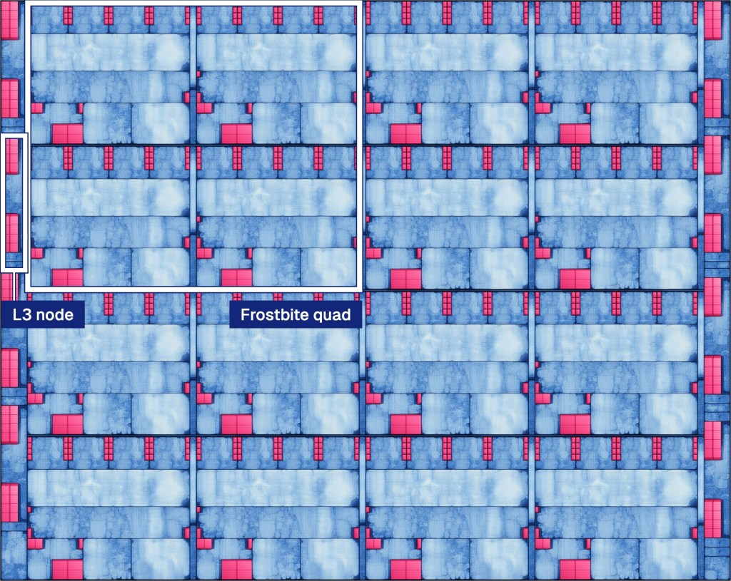
A named, openly inspectable CPU baseline is missing: the company says it cannot disclose the comparison chip for legal reasons. Some benchmark kernels were scaled down substantially, and larger industry tests such as SPEC and PARSEC are still planned. Power estimates were aligned with RTL simulations, but no physical chip has yet established the stated energy savings in silicon.
AI design is moving beyond circuit optimization
Frostbite’s development workflow is arguably as significant as its proposed architecture. Architect Labs says AI agent swarms explored 58 design ideas and retained 37, checking changes against formal specifications. Its ASL language translates into Lean proofs, with more than 800,000 lines of generated verification material reported across the project.
The distinction from existing industrial efforts matters. OpenAI and Synopsys have worked on AI-assisted chip-design tools, while IBM has pursued two instruction-set architectures on a single CPU core. Frostbite instead proposes redesigning the computational model along with the hardware.
What must happen before it becomes a real CPU?
Architect Labs says it intends to release the Frostbite RTL and ISA, demonstrate a software playground on FPGAs, and develop a preliminary operating system. Until then, Frostbite cannot be treated as a drop-in alternative to mainstream Arm or x86 server chips such as those used in Microsoft’s Cobalt 200 cloud platform. Compiler support, application compatibility, physical power measurements, reliability, and reproducible third-party benchmarks remain unresolved.
Even with those limits, Frostbite raises a consequential question: could future processors abandon some of the shared-memory assumptions engineers have optimized for decades? The answer will depend on working silicon, software tooling and independent performance tests—not simulations alone.
Primary documentation: Architect Labs, Frostbite technical disclosure (November 18, 2026); Yves Lafont, “Interaction Nets,” POPL 1990; OpenAI, Advancing chip design (November 18, 2026); Reuters, company funding background (June 18, 2026).


Leave a Reply