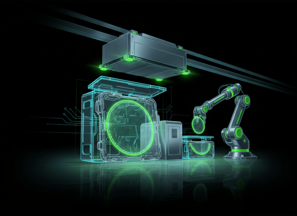
Semiconductor wafer handling is a precision material-control discipline. The objective is to move wafers between carriers, load ports, robots, process tools, storage systems, and metrology stations without adding particles, scratches, electrostatic risk, mechanical damage, or traceability errors.
OSSTC.002 continues the technician foundation established in OSSTC.001: Semiconductor Fab Cleanroom, Contamination, and ESD Basics. The technician-level handling concepts also connect to the device and process perspective introduced in OSSEC.001: Semiconductor Device Physics, Band Gaps, Doping, and PN Junctions.
Wafer handling is part of the manufacturing process
A semiconductor wafer passes through many process and inspection steps before completed die can be tested and packaged. Between those steps, the wafer must be transported, identified, aligned, loaded, unloaded, stored, and transferred with controlled contact and repeatable positioning.
Handling is therefore not separate from yield. A process recipe may be correct while product is still damaged by an incorrect slot assignment, contaminated carrier, robot collision, edge contact, alignment error, static event, or traceability mistake.
- Product protection: prevent particles, scratches, breakage, and electrostatic effects.
- Position control: place each wafer where the tool expects it.
- Identification: preserve lot, carrier, wafer, and process history.
- Automation: transfer material repeatably between tools and storage locations.
- Safety: keep personnel clear of moving robots, hoists, doors, and automated transfer zones.
Why wafers require controlled handling
A finished or partially processed wafer can represent many hours of manufacturing time and a large amount of accumulated process value. Its surface contains structures that may be vulnerable to particles, chemical residue, electrostatic attraction, mechanical contact, or improper environmental exposure.
The wafer edge also matters. Chipping, cracking, and edge damage can create particles or lead to later breakage. Vacuum end effectors, edge-grip systems, Bernoulli systems, electrostatic chucks, and other handling methods are selected according to the process, wafer condition, equipment design, and contamination requirements.
Entegris describes wafer-handling systems as contamination-control and product-integrity tools used during processing, storage, and transport throughout semiconductor manufacturing.
FOUP fundamentals
FOUP means Front Opening Unified Pod. In a modern 300 mm fab, the FOUP is a closed wafer carrier designed to interface with automated transport systems and process-tool load ports while reducing exposure to the surrounding environment.
A FOUP performs several technician-critical functions:
- Holds wafers in defined slot positions.
- Provides a repeatable mechanical interface to compatible load ports.
- Reduces direct environmental exposure during transport and storage.
- Supports automated identification and material tracking.
- Allows automated material-handling equipment to move wafer lots without routine manual carrying.
Entegris documents the development of the FOUP from earlier open cassettes and SMIF-based transport toward standardized front-opening carriers for 300 mm manufacturing.
FOUP condition is a process condition
A FOUP should not be treated as ordinary storage. Carrier condition can affect contamination control, wafer positioning, tool interfacing, and automation reliability.
- Doors, latches, kinematic interfaces, and contact surfaces must remain within specification.
- Carrier interiors must remain within approved cleanliness requirements.
- Slot damage or deformation can interfere with wafer placement and mapping.
- Identification hardware and tracking data must correspond to the correct material.
- Unapproved cleaning materials, lubricants, labels, or repairs can create contamination or mechanical problems.
Carrier inspection and cleaning procedures are site-specific. A technician should follow the approved carrier-control procedure rather than improvising a repair or cleaning method.
Video 1: Precision wafer-transfer automation
Load ports connect the carrier to the tool
The load port is the mechanical and automation interface between the wafer carrier and the process tool. A FOUP is positioned and docked at the load port so the tool can establish the controlled transfer path required for wafer movement.
Typical load-port functions can include carrier detection, docking, clamping, door opening, identification, mapping support, interlock confirmation, and communication with the equipment control system.
A load-port alarm should be treated as a controlled equipment condition. Misalignment, obstruction, door-state disagreement, carrier-detection faults, mapping faults, or mechanical interference can indicate conditions that require product protection before reset or recovery.
EFEM: the atmospheric transfer zone
Many semiconductor tools use an Equipment Front End Module, commonly abbreviated EFEM. The EFEM forms the controlled atmospheric transfer section between the load ports and the process equipment.
Depending on the tool, the EFEM can contain one or more wafer-handling robots, aligners, mapping sensors, environmental controls, and interfaces to load locks or process modules.
- Load port: receives and docks the carrier.
- Robot: transfers wafers between defined positions.
- Aligner: establishes orientation or centering as required.
- Mapping system: determines occupied and empty wafer slots.
- Tool interface: passes wafers toward the process path.
Wafer mapping and slot discipline
Automated tools must know which carrier slots contain wafers and whether the wafers are positioned correctly. Mapping systems detect slot occupancy and can identify conditions such as cross-slotting, double-slotting, protrusion, or unexpected wafer position depending on equipment capability.
Slot discipline is a traceability requirement as well as a mechanical requirement. A wafer transferred under the wrong slot identity can create incorrect process history even when no physical damage occurs.
The robot does not merely move from point A to point B
Semiconductor wafer robots operate through taught or calibrated positions that define safe transfer paths. Motion must account for wafer diameter, carrier geometry, end-effector geometry, tool clearances, door state, chamber state, and interlocks.
Robot calibration errors can produce several failure modes:
- Wafer edge contact.
- Scratches or particle generation.
- Misplacement on a chuck or stage.
- Cross-slotting in the carrier.
- Collision with a door, aligner, chamber, or cassette feature.
- Vacuum pickup failure.
- Wafer drop or breakage.
Recovery from a robot fault should follow the equipment recovery procedure. Manual movement of robot axes or wafers without the documented recovery method can convert a recoverable fault into product damage or equipment damage.
Automated Material Handling Systems
AMHS means Automated Material Handling System. In a highly automated fab, AMHS coordinates carrier movement between process tools, metrology equipment, stockers, buffers, and other destinations.
One common implementation is overhead transport, where automated vehicles move FOUPs above the cleanroom floor. Other systems can include stockers, conveyors, local buffers, and automated transfer stations. The exact architecture varies by fab.
AMHS improves repeatability and reduces routine manual carrier handling, but it also introduces equipment that must be treated as energized automation. Hoists, moving vehicles, lifts, stockers, doors, and transfer mechanisms can create pinch, crush, drop, and struck-by hazards.
Video 2: Wafer fabrication and fab flow
Material tracking and lot identity
Physical movement and digital movement must agree. Manufacturing execution systems and equipment-control systems can associate a carrier with a lot, route, recipe, process step, tool, wafer identity, and status.
A material-handling error can therefore occur without any broken wafer. Examples include the wrong carrier at the wrong tool, incorrect lot status, process-route mismatch, wafer-slot mismatch, or a carrier identity that does not correspond to the expected production material.
The technician response to an identity or routing discrepancy should preserve traceability. Product should not be moved merely to clear an alarm unless the approved recovery process establishes the correct material state.
Alignment and orientation
Wafers may require a known rotational orientation before a process or inspection step. Alignment systems can use edge features, notches, image recognition, or other methods to establish position and orientation.
Centering is equally important. A wafer that is not centered can create transfer problems, chucking errors, measurement errors, or process nonuniformity depending on the tool.
Vacuum handling and end effectors
Many atmospheric wafer robots use vacuum-based end effectors. A controlled vacuum holds the wafer during transfer. The system must detect pickup and release correctly, and the end effector must remain clean, undamaged, and calibrated.
Vacuum-related transfer faults can involve leaks, contamination, damaged tubing, sensor faults, incorrect pickup position, surface condition, warped wafers, or end-effector wear. Random adjustment of vacuum thresholds or robot positions can mask the actual problem and should not substitute for documented troubleshooting.
Handling warped, thinned, or fragile wafers
Advanced packaging, compound semiconductors, power devices, temporary bonding, thinning, and other processes can produce wafers that require specialized handling. Mechanical stiffness, bow, warp, backside condition, and edge condition can change the acceptable transfer method.
The existence of specialized non-contact, edge-grip, and low-stress handling systems reflects a central technician principle: wafer handling must match the physical state of the material rather than assuming every wafer behaves like a rigid flat disk.
Video 3: Complete microchip manufacturing context
Process equipment depends on clean transfer interfaces
ASML describes semiconductor manufacturing as a sequence in which robots move wafers from machine to machine through tightly controlled fab environments. ASML’s manufacturing overview shows how repeated deposition, lithography, etch, and related steps depend on stable wafer movement between tools.
The practical implication is that a transfer fault can interrupt far more than one robot. It can block a tool, stop a lot, trigger queue delays, require product disposition, or create downstream uncertainty about wafer condition.
Technician response to a wafer-transfer fault
- Stop or hold the equipment according to the documented fault procedure.
- Determine whether a wafer is on an end effector, stage, aligner, chamber interface, or carrier slot.
- Preserve the reported slot, lot, and carrier identity.
- Review alarm history and the last completed robot motion.
- Verify door, vacuum, mapping, and position states according to the tool procedure.
- Do not command additional automatic motion until the wafer location and collision risk are known.
- Use the approved recovery mode or maintenance procedure if intervention is required.
- Inspect for particles, chips, scratches, broken wafer fragments, or mechanical interference as authorized.
- Return the tool to production only after transfer state, carrier state, and material identity are verified.
Broken-wafer response
A broken wafer is both a product event and a contamination event. Fragments can remain in a carrier, robot path, aligner, load lock, chamber interface, or process module.
Recovery should prevent additional automated motion from spreading fragments. The approved broken-wafer procedure should define isolation, cleanup, inspection, verification, and product disposition. Bare-hand collection, compressed-air blowing, or improvised vacuuming can create additional hazards or contamination and should not replace the site procedure.
Wafer-handling safety
Automated handling equipment can move quickly and may restart after an interlock or fault condition is cleared. Technician work around robots, load ports, stockers, and AMHS equipment therefore requires strict control of stored energy and automatic motion.
- Do not reach into an automated transfer envelope merely because motion has stopped.
- Do not defeat door, carrier, robot, or load-port interlocks outside an approved procedure.
- Apply required lockout/tagout or service modes before entering hazardous motion zones.
- Account for pneumatic, vacuum, gravity, spring, and electrical energy in addition to motor power.
- Use approved wafer-recovery and carrier-handling tools.
Common technician mistakes
- Handling a carrier as ordinary storage rather than process equipment.
- Moving a wafer manually before confirming its slot and lot identity.
- Resetting a robot repeatedly without determining wafer location.
- Ignoring small chips or edge damage because the wafer remains intact.
- Cleaning a FOUP or end effector with unapproved materials.
- Changing robot coordinates without documenting the original calibration state.
- Assuming a transfer fault is purely mechanical when mapping, identification, vacuum, or software state can also be involved.
- Entering an automated motion zone without controlling restart energy.
Exercises
- Draw a process-flow sequence containing a FOUP, load port, EFEM robot, aligner, process module, and return to the carrier.
- List five failure modes that can prevent a wafer from being transferred safely from a FOUP to a tool.
- Describe the difference between a material-identification fault and a mechanical transfer fault.
- Explain why repeated reset commands can increase risk after a robot transfer fault.
- Identify the controls required before entering the motion envelope of an automated wafer-handling robot.
- Compare vacuum pickup, edge-grip, and non-contact handling at a conceptual level and identify one situation in which each method could be useful.
- Write a recovery checklist for a wafer found partially outside its expected carrier slot.
Knowledge check
1. What does FOUP mean?
Front Opening Unified Pod.
2. What is the purpose of a load port?
It provides the controlled mechanical and automation interface between a wafer carrier and process equipment.
3. What is an EFEM?
An Equipment Front End Module that provides atmospheric wafer transfer between load ports and the process path.
4. Why is wafer mapping important?
It establishes carrier slot occupancy and helps identify incorrect wafer positions before transfer.
5. What does AMHS mean?
Automated Material Handling System.
6. Why must physical material movement and digital tracking agree?
Correct processing depends on preserving lot, carrier, wafer, route, and process-history identity.
7. Why can a broken wafer affect equipment beyond the original break location?
Fragments can spread through robot paths, carriers, aligners, load locks, and process interfaces if motion continues.
8. What is the correct general response to an unknown wafer position after a robot fault?
Stop uncontrolled motion, establish the wafer location and equipment state, preserve material identity, and use the approved recovery procedure.
Key takeaway
Wafer handling combines contamination control, precision robotics, carrier discipline, automation, traceability, and safety. FOUPs protect and organize wafers, load ports connect carriers to tools, EFEM robots perform precise transfer, and AMHS moves material across the fab. Reliable manufacturing requires every physical wafer movement to remain mechanically controlled and digitally traceable.
Display note: this lesson uses standard Gutenberg paragraphs, lists, tables, headings, and media embeds only. No decorative text-box or callout-box layout is used.
BitcoinVersus.Tech
Advertisement
Editor’s Note:
We volunteer daily to ensure the credibility of the information on this platform is Verifiably True. If you would like to support our research initiatives, please donate here: 3C9o19EH5HSiwEPyCTmEKzxhNCbo2X6TTb
BitcoinVersus.tech is not a financial advisor. This media platform reports on financial subjects purely for informational purposes.


Leave a comment