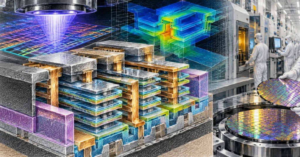
IBM and Siemens are teaming up to push IBM’s 3D nanostack transistor architecture closer to practical manufacturing. The companies announced October 14 that Siemens will contribute electronic-design automation, process simulation, lithography optimization and manufacturing software to help IBM model and refine future nanostack generations.
IBM’s new collaboration announcement says nanostack vertically stacks and staggers nanosheet transistors rather than relying only on shrinking them laterally. IBM says its current 7-angstrom research node can place nearly 100 billion transistors in a fingernail-sized area.
TechTechPotato explains IBM’s 7-angstrom nanostack architecture and how it differs from conventional nanosheet scaling.
IBM’s earlier nanostack research disclosure described the architecture as a route beyond ordinary gate-all-around scaling. The new work with Siemens focuses on the harder next step: building virtual models, optimizing lithography and identifying fabrication problems before chips reach a manufacturing line.
The architecture builds on the same electrostatic ideas covered in gate-all-around nanosheet electrostatics, but moves further into vertical transistor stacking. It also fits the broader shift toward angstrom-scale process control and the race to commercialize next-generation logic manufacturing. IBM has demonstrated the research architecture, but this announcement is not a commercial production launch.
BitcoinVersus.Tech Editor’s Note:
We volunteer daily to ensure the credibility of the information on this platform is Verifiably True. If you would like to support to help further secure the integrity of our research initiatives, please donate using the QR code provided

For best QR-code scanning results, please scan this donation code from a desktop or larger screen. Mobile screens may prevent camera recognition.
BitcoinVersus.Tech provides technical education and analysis for informational purposes only.


Leave a Reply