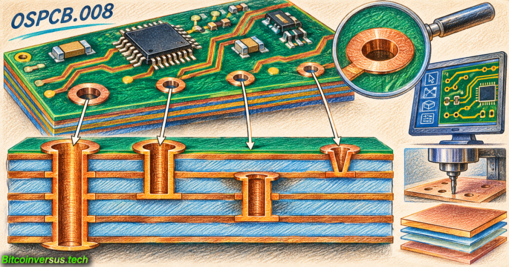
OSPCB.008 explains how PCB vias survive fabrication. The topic follows KiCad’s October 30, 2026 version 10.0.8 maintenance release, which fixed a crash involving boards containing via padstacks and an input-handling problem in the via-style rule editor. Those were software fixes, not proof that every via geometry is manufacturable.
Altium Academy, “Mechanically Drilled Blind & Buried Vias: PCB Design Rules Explained,” September 11, 2025. Manufacturer-supported instruction covering lamination and drilling limits; Altium interface demonstrations are not KiCad procedures.
What a via connects
A through-via spans both outer copper surfaces. A blind via connects an outside layer to one or more inner layers. A buried via joins inner layers without reaching an outer surface. A microvia is typically laser-drilled for short layer transitions in high-density interconnect construction. Layer span and fabrication sequence must match the actual board stackup.
Review OSPCB.002 on pads and vias and OSPCB.001 on copper stackups before choosing advanced structures.
Two calculations engineers must not confuse
Nominal annular ring: For an illustrative circular 0.60-mm copper pad and a 0.30-mm hole, (0.60 − 0.30) ÷ 2 gives a 0.15-mm radial ring if perfectly centered. Drill wander, pad registration, plating and the difference between drilled and finished-hole diameters can reduce real finished copper. Fabricator tolerances determine acceptability.
Mechanical drill aspect ratio: A hypothetical 1.60-mm board drilled with a 0.30-mm bit gives 1.60 ÷ 0.30 ≈ 5.3:1. Aspect ratio uses the drilled depth and mechanical drill diameter, not an arbitrary finished-hole opening. Blind-via depth is smaller than full board thickness. The two numerical cases are separate teaching examples, not a released PCB design.
Configure KiCad 10 for real fabrication
- Obtain the fabrication house’s approved stackup, minimum drill sizes, annular-ring limits and permitted layer spans before selecting via styles.
- In Board Setup, configure physical stackup and design-rule constraints. Set board-level minimum annular width, hole-to-hole spacing and via dimensions from the quoted process capability.
- For a training design, start routing a track with X; V places a through-via, Ctrl+V places a microvia, and Alt+Shift+V places a blind or buried via, subject to configured routing and layers.
- Inspect the selected via’s diameter, hole and layer span. Run Inspect → Design Rules Checker and resolve annular-width, hole-size and clearance errors.
- Export approved Gerber layers and drill files, or an accepted IPC-2581/ODB++ package. Verify plated versus non-plated drill outputs, layer ordering and fabrication notes with the board house.
KiCad’s version 10 PCB Editor manual documents the via hotkeys, design-rule checks and Excellon drill outputs. A clean DRC cannot independently validate plating thickness, registration, buried-via lamination yield or the fabrication vendor’s capabilities. The companion OSPCB.004 routing lesson explains why configured design limits matter.
Altium Academy, “How to Use Blind and Buried Vias,” July 14, 2023. Layer-transition tradeoffs and stacked versus staggered routing; actual production requirements vary by fabricator.
The engineering tradeoff
Through-vias are widely supported, while advanced buried, blind and microvia structures can free dense routing channels but add fabrication steps, cost and yield considerations. Via-in-pad structures may require specified filling and capping rather than exposed openings. For fast digital interfaces, layer changes can also disrupt the reference path; review OSPCB.007 signal integrity and OSPCB.006 decoupling layout.
Knowledge check
Does a 0.15-mm nominal annular ring guarantee 0.15 mm after drilling? No. Does every microvia cross the full PCB? No. Does passing DRC authorize fabrication? No. Approve designs only after reviewing the manufacturer’s process limits and output package.
Primary references: KiCad October 2026 release notes; KiCad 10 PCB Editor manual; Phil’s Lab / Altium via sizing guide; Altium design-for-manufacturing overview.
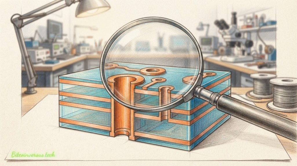
Editor’s Note: OSPCB.008 follows the two published OSPCB.007 chapters without repeating their differential-routing lessons. KiCad’s October 30 release confirms the via-padstack crash and via-style input fixes. The ring and aspect-ratio calculations are hypothetical and were not measured on a manufactured board. The original 1200 × 630 cover and explanatory in-story image are conceptual artwork, not inspection evidence. Both Altium Academy videos have identifiable public pages, titles and channels; in-page playback and fabrication accuracy remain separate verification steps. No physical board, production order, plated-barrel section or drill file was tested.

To scan on a phone, display the QR on a second screen and scan using a compatible Bitcoin wallet. Certain wallets can also read a saved QR image on the same phone. Verify the address 3C9o19EH5HSiwEPyCTmEKzxhNCbo2X6TTb and the 5,000-satoshi amount before sending. Bitcoin transfers are generally irreversible.
We volunteer daily to ensure information published by BitcoinVersus.Tech is Verifiably True. Optional donations support independent research and technical education. Content is educational, not a substitute for fabricator approval, certified engineering review, financial advice or individualized professional guidance.


Leave a Reply