OSPCB.002 — Open-Source Printed Circuit Board | Foundational Lesson
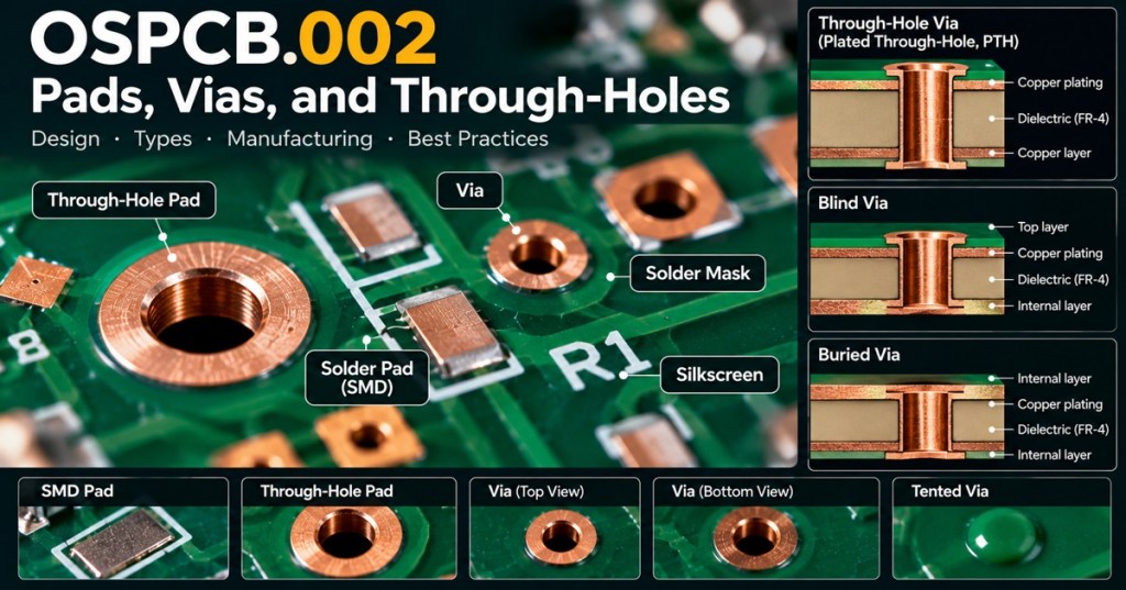
Pads and vias are among the smallest features on a printed circuit board, but they perform essential jobs. Pads provide conductive attachment points for components, while vias connect copper between board layers. This lesson explains how to identify each feature and why a hole in a PCB is not automatically an electrical connection.
Learning Objectives
- Distinguish a surface-mount pad from a plated through-hole pad.
- Explain the purpose of through, blind and buried vias.
- Recognize that mechanical mounting holes may be nonplated.
- Identify how solder mask and copper annular rings affect visible board features.
Pads Attach Components
A surface-mount device (SMD) pad is an exposed copper land where a component terminal can be soldered to the board. A through-hole pad surrounds a hole into which a component lead is inserted; when plated, the hole barrel can connect to copper on other layers. A pad’s dimensions, spacing and solder-mask opening must match the component and manufacturing process. The KiCad PCB Editor manual explains pad types, footprints and their electrical net assignments.
Phil’s Lab explains how copper tracks and pads are used in PCB layout. This is background instruction, not a demonstration of every via construction method.
Vias Connect Copper Layers
A through-via passes through the board and commonly connects outer and selected internal copper layers. A blind via connects an outer copper layer to one or more inner layers without passing through the entire board. A buried via joins internal layers and is not exposed on the finished board surfaces. These structures have different fabrication costs and constraints. The presence of a via does not mean it connects to every copper layer it passes: layer connections depend on the copper geometry and design.
A visible ring of copper surrounding a plated hole is called an annular ring. Some vias are tented under solder mask; others are exposed, plugged or filled depending on manufacturing requirements. Beginners should not assume that a covered hole is absent or that a large mounting hole is plated.
Through-Holes Versus Mounting Holes
A through-hole component pad is intended for electrical assembly. A mechanical mounting hole is primarily for a fastener or standoff and may be plated or nonplated according to the design. A plated mounting hole can be intentionally tied to chassis or ground, but that must be confirmed from the schematic, PCB layout or continuity measurements on safely isolated hardware. A visual inspection alone cannot prove the electrical connection.
For a broader visual explanation, see SparkFun’s PCB Basics guide. Our earlier lessons introduce PCB construction in OSPCB.000 and copper stackups in OSPCB.001. The KiCad schematic-to-board update explains how design software carries electrical connections into a board layout.
Related community design review shows how pads, copper routing and board features can change between revisions. Community posts are not formal manufacturing specifications.
Five-Minute Identification Exercise
Safety: use an unpowered, disconnected practice PCB. Avoid mains-powered devices, batteries and power supplies with charged capacitors. Do not solder or apply power during this exercise.
- Find one exposed rectangular SMD pad and note its position.
- Find a hole surrounded by copper and determine whether it resembles a through-hole component pad or a via.
- Locate a mechanical mounting hole, if present, and note whether a copper ring is visible.
- Look for any solder-mask-covered vias. Record what you can see and what cannot be confirmed without documentation.
- Sketch the difference between a through-via and a blind via in a four-layer board.
Knowledge Check
- What is the primary job of an SMD pad?
- How does a blind via differ from a through-via?
- Must every mounting hole carry an electrical signal?
- What is an annular ring?
Answers: An SMD pad provides a conductive attachment for a surface-mounted terminal. A blind via reaches an outer layer and some inner layers without passing through the entire board; a through-via passes through the board. No, mounting holes may be electrically isolated. An annular ring is the copper surrounding a plated hole.
Conclusion
Pads attach electronic parts; vias link selected copper layers; and mechanical holes support assembly. Understanding these distinctions prepares students to inspect footprints and read PCB layout files. The next lesson can explore component footprints and land patterns in more detail.
BitcoinVersus.Tech Editor’s Note: We volunteer daily to ensure the credibility of the information on this platform is Verifiably True. If you would like to support to help further secure the integrity of our research initiatives, please donate using the QR code provided

For best QR-code scanning results, please scan this donation code from a desktop or larger screen. Mobile screens may prevent camera recognition.


Leave a Reply