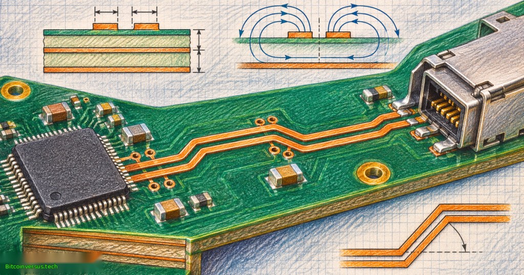
OSPCB.007 moves from power integrity to signal integrity: how do two high-speed PCB traces preserve their intended timing and impedance between chips and connectors? Differential signaling sends complementary electrical waveforms over a pair of conductors. Receivers respond to the voltage difference, improving tolerance to certain common-mode disturbances. Geometry, dielectric materials, termination and reference-plane continuity still determine whether a physical link performs reliably.
Altium Academy, “What Are Differential Pairs?” (September 29, 2021). Zach Peterson introduces differential signaling, impedance and reference-ground considerations. Credit: Altium Academy / YouTube.
Begin with the full transmission path
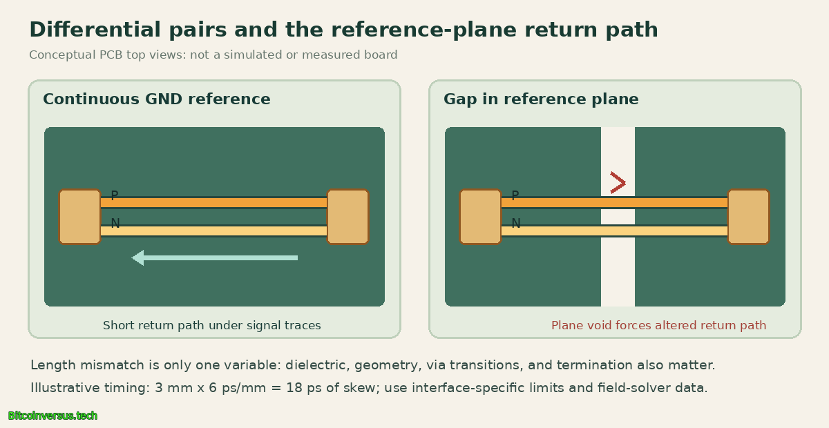
A differential pair is not simply two nearby traces. The transmitter, receiver, connector, dielectric stackup, copper geometry and terminating circuitry form a transmission system. The pair may carry equal-and-opposite components, yet nearby ground planes can still carry substantial return currents. Routing across a cut or void in the reference plane creates a discontinuity and can increase electromagnetic emissions or degrade the signal.
Review OSPCB.005 on return-current paths and OSPCB.006 on decoupling. Both principles remain essential even when a high-speed interface uses differential signaling.
Impedance is a stackup property
A trace’s characteristic impedance depends on its width, copper thickness, height above a reference plane and effective dielectric constant. The pair’s differential impedance additionally depends on spacing and coupling. A target such as 90 Ω or 100 Ω must come from the applicable interface and component specifications, not a universal PCB rule. Ask the fabricator for the approved layer stackup and controlled-impedance geometry before fixing trace widths.
Keep the pair’s spacing and reference environment consistent through the principal route; minimize stubs, needless vias and abrupt transitions. Connector breakouts can require different geometry. A continuous reference plane is normally preferable to routing across gaps, although the final requirements depend on the actual interface.
Timing example: trace length is not the whole answer
Suppose one conductor is 3 mm longer than the other and an illustrative propagation delay is 6 ps/mm. The additional one-way delay is 3 × 6 = 18 ps. The calculation is arithmetic, not a measured interface skew; actual delay depends on dielectric, stackup and conductor geometry. Package and connector delays may also contribute. The permitted mismatch must come from the specific device and protocol requirements.
Length tuning can solve a documented skew problem, but adding excessive serpentine routes may introduce coupling and impedance variation. Equal geometric trace length alone cannot establish acceptable eye opening, insertion loss, crosstalk, or electromagnetic compatibility.
KiCad 10 practice workflow
Ampnics, “How to use differential pair tracks in KiCAD | Part 25” (August 31, 2025). Demonstrates differential-pair naming, routing and tuning; shown as a software tutorial rather than verification of the example board. Credit: Ampnics / YouTube.
- Open a non-energized training design and label schematic nets with consistent complementary suffixes such as USB_P and USB_N.
- Read the actual IC datasheet and interface design guide to determine impedance, allowable skew, termination and layer recommendations.
- In Board Setup, configure the stackup and net classes; obtain a manufacturer-approved trace width and pair gap.
- Start Route Differential Pair or press 6. Inspect the positive and negative tracks as a coupled route rather than judging only visual symmetry.
- Retain a continuous reference plane and inspect each breakout, layer change and via pair for unwanted discontinuities.
- Use differential-pair length tuning (8) or skew tuning (9) only where justified by measured or specified requirements.
- Refill copper zones, check the routing against OSPCB.004 design-rule guidance, and run Inspect → Design Rules Checker.
- Document assumptions, review the stackup and via design, then arrange simulation or laboratory validation when appropriate.
KiCad can check configured gap, length, skew and clearance constraints, but its router cannot independently prove the manufacturer’s actual impedance tolerance or full signal performance. A correct fabricator stackup, interface-specific limits, field-solving or simulation, and appropriate laboratory measurements remain separate engineering steps.
Knowledge check
Question: Can two equal-length traces still violate signal-integrity requirements? Answer: Yes. Incorrect impedance, discontinuous return paths, connector effects and excess loss can all cause failure. Question: Is 100 Ω a mandatory differential impedance for every interface? Answer: No. Use the component and protocol specifications.
Primary technical references: KiCad 10 PCB Editor manual (differential-pair routing, length and delay tuning, design rules); Texas Instruments, High-Speed Interface Layout Guidelines, Rev. J; Texas Instruments, High-Speed Layout Guidelines for Reducing EMI for LVDS SerDes Designs; and the two identified instructional videos. Source recommendations are interface-dependent; the 18 ps example uses a declared illustrative propagation factor.
Editor’s Note: OSPCB.007 follows OSPCB.006 and extends the site’s open-source printed-circuit-board curriculum. Manufacturers’ application guidance and the KiCad 10 reference manual support the routing discussion. The 3 mm/18 ps example is hypothetical; no field solver, device-specific design, oscilloscope or fabricated board was tested. The 1200 × 630 colored-pencil cover and separate educational diagram are original conceptual artwork with neon-green Bitcoinversus.tech identification. Video identities and public watch pages were checked; actual playback, live mobile layout and embedded-player permissions require independent verification.

BitcoinVersus.Tech is volunteer-run and publishes independent technical education. An optional 5,000-satoshi donation helps support research. Scan the original QR from a second screen using a compatible Bitcoin wallet; on the same phone, use a wallet able to import a saved QR image if supported. Independently verify recipient 3C9o19EH5HSiwEPyCTmEKzxhNCbo2X6TTb and the amount before payment. Bitcoin transfers are generally irreversible.
We volunteer daily to ensure the information on BitcoinVersus.Tech is Verifiably True. Educational coverage does not constitute individual engineering certification, manufacturing approval, financial advice or investment advice.


Leave a Reply