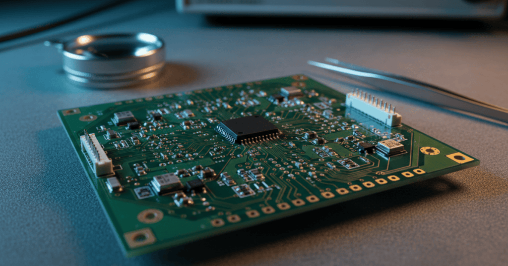
A printed circuit board does more than hold electronic parts. Its patterned copper forms the electrical routes between component terminals. After defining the stackup, pads, vias and footprints, an engineer must connect the intended nets while preserving copper spacing, manufacturability, signal integrity and adequate conductor dimensions. The layout stage transforms a schematic’s logical connections into physical metal.
OSPCB.004 builds on OSPCB.003 — Component Footprints and Land Patterns, OSPCB.002 — Pads, Vias and Through-Holes, and OSPCB.001 — PCB Layers and Copper Stackups. The current chapter introduces the trace, the meaning of width and clearance, design-rule checking (DRC), and how an interactive router keeps a layout inside approved board rules.
Learning Objectives and Prerequisites
- Distinguish a net from a copper track, a segment, a via, a copper zone and a footprint pad.
- Explain why trace width affects conductor resistance and heating, and why a simple resistance calculation cannot determine allowable current alone.
- Define copper-to-copper clearance as an edge-to-edge distance, distinct from center-to-center pitch and from board-edge clearance.
- Interpret hypothetical routing rules without mistaking illustrative dimensions for universal fabrication limits.
- Describe KiCad 10’s interactive routing modes, net classes, board setup, and DRC workflow.
- Calculate simplified trace cross-sectional area, resistance, voltage drop and I²R dissipation for known dimensions.
- Run a documentation-based PCB review and record unresolved fabrication, insulation or signal-integrity requirements before release.
Prerequisites include a schematic netlist, correctly assigned footprints, the distinction between top and bottom copper layers, and the basic meaning of resistance in ohms. The introductory printed-circuit-board lesson supplies the earlier vocabulary. No electrical power, soldering, chemical processing or live board measurement is required for the training exercise.
The Net Is Logical; the Trace Is Physical
In schematic capture, a net is a named electrical connection among pins. In a PCB editor, the corresponding pads are often joined by narrow copper tracks and, when necessary, plated vias that carry the connection to another copper layer. The short graphical lines that show connections needing routing are often called ratsnest or airwires. They are visual reminders, not metal conductors and not finished board routes.
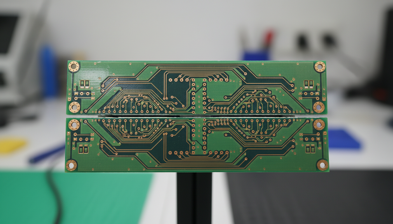
A track can consist of several line segments. The trace width is the physical copper width measured perpendicular to its local path. A copper zone fills a region and may connect many pads to the same net; its relationships to other nets must also meet clearance rules. A via changes layers, but also adds geometry, manufacturing cost and electrical effects. The most direct route is not automatically the best route if it cuts through the required return path or approaches another net too closely.
The KiCad 10 PCB Editor documentation specifies that the interactive router uses net-class width and board design rules. Its default routing modes are designed to preserve clearance rules while placing or moving tracks, with deliberately permissive options available for advanced users. Beginners should not disable DRC protections to make a crowded route fit.
Trace Width, Copper Thickness, and Cross-Sectional Area
A simplified rectangular track has cross-sectional area A = w × t, where w is width and t is the finished conducting copper thickness. Thin PCB copper is commonly described using nominal copper weight, such as one ounce per square foot (often approximated as 35 µm thickness for elementary calculations). Finished conductor thickness and manufacturing tolerances may differ from the nominal foil specification.
Electrical resistance at a chosen reference temperature follows R = ρL/A in an ideal uniform conductor, where ρ is material resistivity and L is length. Geometry matters: doubling the width, with the same material and thickness, doubles cross-sectional area and halves modeled DC resistance. Increasing length in the same ratio increases resistance. A via, connector, narrow pad transition, or solder joint may contribute additional resistance beyond the ideal straight trace.
Use the following hypothetical copper route, with uniform cross-section and a room-temperature copper resistivity approximated as 1.68 × 10⁻⁸ Ω·m. All quantities must be converted to compatible SI units before evaluating the equation:
Length L = 50 mm = 0.050 m
Width w = 0.25 mm = 0.00025 m
Copper thickness t = 35 µm = 0.000035 m
Area A = w × t = 8.75 × 10⁻⁹ m²
ρ = 1.68 × 10⁻⁸ Ω·m
R = ρL / A = 0.096 Ω
At a hypothetical direct current of 0.50 A, the modeled voltage drop is ΔV = I × R = 0.048 V, or 48 mV. Its dissipated power is P = I²R = 0.024 W, or 24 mW. If width increases to 0.50 mm while all other assumptions remain unchanged, the modeled trace resistance falls to 0.048 Ω, the drop to 24 mV, and dissipation to 12 mW.
Width 0.25 mm: R = 0.096 Ω; ΔV = 0.048 V; P = 0.024 W
Width 0.50 mm: R = 0.048 Ω; ΔV = 0.024 V; P = 0.012 W
The calculation was checked numerically; it is an ideal geometric comparison, not a safe current rating. Copper resistance rises with temperature; conductor heating depends on nearby copper, board construction, airflow, component heat, waveform, and acceptable temperature rise. The IPC-2152 design standard addresses current-carrying capacity through the interaction of conductor dimensions and thermal conditions. Published current-capacity tables or calculators should be used only with correct assumptions and design validation.
What Counts as Copper Clearance
Clearance ordinarily describes the shortest permitted separation between two conductive objects on different nets. It is measured from copper edge to copper edge, not between the centers of traces. For example, two straight 0.25 mm-wide parallel traces separated by an edge clearance of 0.20 mm have a center-to-center distance of 0.25 + 0.20 = 0.45 mm when they have equal widths.
A net’s required electrical clearance can depend on voltage, insulation standards, expected pollution environment, manufacturing process and the applicable product safety rules. A 0.20 mm clearance may be adequate for some low-voltage manufacturer capabilities but is emphatically not a blanket instruction for mains, high-voltage, medical, automotive, safety-isolated or other controlled circuits. Creepage follows an insulating surface path, while clearance in insulation coordination can refer to the shortest distance through air. PCB tool fields also include specialized copper-clearance constraints; read the applicable rule type rather than treating all distances as equivalent.
Consider an illustrative low-voltage design in which a selected fabricator confirms a 0.20 mm minimum copper separation. A proposed 0.15 mm gap would miss that stated constraint by 0.05 mm. The correct response is not to suppress the violation; it is to reroute, change placement, or obtain an approved alternative manufacturing rule. Board-edge spacing, drill-to-copper, copper-to-hole and solder-mask sliver constraints are separate checks.
KiCad 10 Router and Design-Rule Workflow
The KiCad PCB Editor provides board-wide constraints, net-class defaults and custom rules. Values must be derived from actual fabrication capabilities and circuit requirements. KiCad’s version 10 PCB editor manual describes board setup, interactive routing, the graphical design-rule editor and DRC reporting. An illustrative beginner workflow proceeds in the following order:
- Verify the schematic and netlist: use the PCB editor’s schematic-update workflow so pads carry the intended net assignments. Review footprint-to-component matching before routing.
- Review the stackup and manufacturer limits: identify copper-layer count, finished copper thickness, allowable track/gap limits, drill sizes, annular rings and edge clearances from the selected fabricator.
- Set board constraints: configure Board Setup and the relevant net classes. A wide high-current supply net may require different preferred widths than ordinary low-current logic signals.
- Place components intentionally: group related parts, allow assembly access and consider the current-return path. Netlines can guide placement, but shortest airwire length is not the only objective.
- Choose a routing width: set a rule-backed preferred size before starting the interactive router. Do not assume the default size suits all nets.
- Route one same-net connection: in the PCB Editor, use the Route Tracks tool or press
X, start from the pad, and follow the highlighted net. KiCad’s Shove and Walk Around modes try to maintain legal separation. - Review vias and zones: confirm that layers connect where intended and that a filled zone has the correct net, clearance and thermal-relief settings.
- Run Design Rules Checker: investigate shorted nets, clearance errors, track-width rule violations, unconnected ends, via connection warnings and manufacturing exceptions.
- Recheck before release: compare the final layout against the schematic and the fabricator’s actual capabilities, then inspect generated manufacturing outputs independently.
EmbeddedU, “KiCad 10 Made Simple From Zero Experience to a Real PCB” (July 27, 2026). The beginner tutorial follows schematic capture, footprint assignment, trace routing, ground zones, DRC and fabrication outputs. The video is instructional; no manufacturing outcome from its example is treated as proof that another PCB will be compliant.
How the Interactive Router Handles Obstacles
In Shove mode, KiCad can move unlocked, movable traces away from a new route where constraints permit. In Walk Around mode, the new track instead navigates around obstacles without relocating existing copper. In Highlight Collisions mode, the editor allows greater manual control and highlights potential violations; the separate option to allow DRC violations should not be used as a routine beginner shortcut.
A valid connection at one zoom level can still fail an end-of-design DRC because a nearby track narrows, a via violates a drill rule, a pad doesn’t connect to its intended net, or a zone fill changes. The interactive router is a design aid—not an independent sign-off against every electrical, thermal, high-speed and factory constraint.
The KiCad 10 DRC rules include different check categories for actual copper shorts, net clearance, track-width limits and unconnected ends. The preferred net-class width can influence how the router draws new tracks, but its preferred value does not automatically set the absolute minimum or maximum permitted width; explicit board or custom rule constraints govern violation checks.

Read an Example DRC Report Correctly
Assume a hypothetical four-net PCB with a general minimum trace width of 0.20 mm, a manufacturer-approved copper gap of 0.20 mm, and a 0.25 mm preferred default routing width. A new trace was narrowed locally to 0.15 mm and another signal track now runs only 0.12 mm from a different-net copper pad. The imagined DRC results should be interpreted as follows:
- Track width rule violation: 0.15 mm is narrower than the specified 0.20 mm minimum, by 0.05 mm.
- Clearance violation: 0.12 mm separation is below the specified 0.20 mm minimum, by 0.08 mm.
- Unconnected item: a pad not yet joined to the intended same-net route may appear as an unconnected warning rather than a copper short.
- Preferred width difference: a trace of 0.22 mm may differ from the 0.25 mm preference but need not violate a 0.20 mm explicit minimum. Determine the actual effective rule before reporting an error.
These are teaching figures, not real DRC logs. The correct workflow is to confirm which rule was applied, inspect the geometry, adjust the routing or constraints through the design approval process, refill copper zones when appropriate, and rerun the full DRC. If a violation is unavoidable, the exception must have an engineering rationale; hiding the error is not an equivalent remedy.
When Simple Trace Geometry Is Not Enough
A PCB track carrying a digital edge, high-current pulse, radio-frequency signal, fast serial pair or sensitive analog signal may require analysis beyond ordinary resistance. Controlled impedance depends on trace width, dielectric thickness and permittivity, copper geometry and the nearby reference plane; a trace’s 50 Ω characteristic impedance is not its DC conductor resistance. Differential pairs can require intentional spacing and skew control. Return-current paths and layer transitions influence signal integrity and electromagnetic emissions.
For higher-current nets, check conductor and via cross section, cumulative voltage drop and thermal response. For switching power stages, verify loop geometry and return paths. For a high-voltage circuit, use relevant insulation rules rather than borrowing low-voltage prototype clearances. For unregulated or safety-related uses, consult a qualified engineer, the actual device requirements and the selected PCB fabrication process before release.
Phil’s Lab, “KiCad 9 Hardware Design Tutorial (TI MSPM0) (2/2 PCB)” (November 28, 2025). The expert layout walkthrough includes power routing, vias, decoupling, mixed-signal routes, DRC and manufacturing files. It uses KiCad 9; interface placement may differ in KiCad 10, whose current documentation governs the steps taught in OSPCB.004.
Five-Minute Documentation Lab
Use a fictitious, unpowered board containing an LED, a series resistor, a small microcontroller and a connector. Do not assume the illustration’s traces are real routed nets. With a schematic or paper sketch, identify the supply, return and signal connections. Assign a net name to each and annotate the intended copper layer.
- List the relevant PCB layer count, copper thickness and hypothetical manufacturer capabilities.
- Define a nominal low-current track width and a separate width candidate for the supply net, documenting why they differ.
- Measure the edge-to-edge distance between two theoretical neighboring tracks and compare it with the selected rule.
- Calculate the ideal resistance of a chosen 50 mm copper trace using the numerical example above, then repeat at twice the width.
- Describe a routing path that avoids a different-net pad, a drilled hole and a board edge, without disabling clearance rules.
- Read a hypothetical DRC warning and distinguish a real violation from a mere change in preferred routing width.
- Write a sign-off note separating validated information from the thermal, signal-integrity, electrical-safety and manufacturer checks still required.
If a learner has KiCad 10 installed, the same exercise may be reproduced in an isolated project and its actual DRC run documented. No live KiCad GUI or PCB project file was created or tested in preparing the lesson, so program-interface guidance is grounded in KiCad’s official manual rather than an asserted execution.
Troubleshooting Common Layout Mistakes
- Routing by appearance only: a visually touching track may belong to the wrong net; use electrical net assignments and DRC.
- Assuming a zero-airwire board must be valid: connected pads can still coexist with shorts, thermal issues or manufacturing errors.
- Confusing clearance with pitch: center-to-center spacing includes trace half-widths; manufacturer rules may specify edge separation.
- Using a universal width for all supply tracks: actual allowable current depends on temperature rise, copper thickness, placement and operating conditions.
- Forcing a trace through an obstacle: inspect routing constraints and component placement before bypassing DRC safeguards.
- Adding a via merely to complete a route: verify drill capability, annular ring, layer connection and its electrical effect.
- Assuming silkscreen and solder mask are copper layers: distinguish manufacturing coating and marking layers from conductive copper.
- Ignoring connection to a plane: ensure each pad has the intended net and appropriate zone connection, thermal relief or direct tie.
- Confusing DC resistance with high-speed impedance: the physical quantities represent different electrical behavior.
Knowledge Check and Explained Answers
- What is the difference between a net and a trace? A net is a logical electrical connection; a trace is physical copper that can implement part of that net.
- What does DRC stand for? Design Rules Checker or design-rule checking: automated checks against defined board constraints.
- Why doesn’t a preferred width always cause a DRC error? The preference can guide routing while separate minimum and maximum constraints determine enforceable width violations.
- What is the cross-section of a 0.25 mm-wide, 35 µm-thick rectangular track? 8.75 × 10⁻⁹ m², using the assumed nominal thickness.
- What is the approximate resistance of the illustrative 50 mm trace? 0.096 Ω under the chosen uniform copper resistivity assumption.
- What happens to the ideal DC resistance if that trace’s width doubles? It halves, as long as material, thickness, temperature and length stay unchanged.
- Why can’t a resistance formula alone assign a safe current rating? Heating, thermal surroundings, allowable temperature rise, manufacturing variation and other factors must be evaluated.
- What can a DRC pass not guarantee? Electrical function, complete safety compliance, signal integrity, adequate thermal performance, real manufacturer acceptance or an actual manufactured board’s quality.
Primary References and Further Reading
Primary sources: KiCad PCB Editor 10.0 documentation for interactive routing, board constraints, net classes and DRC; DLA’s IPC-2152 standard record for the active current-carrying-capacity standard; IPC’s published scope and contents for IPC-2152; and Phil’s Lab PCB routing and design-rule course outlines. Related lessons include OSPCB.002, OSPCB.003 and the site’s KiCad 10 background coverage. All values in the worked examples are hypothetical.
Elementary Conclusion
PCB layout translates a netlist into real copper geometry while applying manufacturing and electrical constraints. Track width affects modeled DC resistance; copper clearance protects separation between incompatible conductors; net classes and routing tools organize the work; and DRC identifies selected rule violations. Successful engineering requires keeping the underlying physical requirements, fabricator limits, thermal behavior and final validation separate from what the editor can automatically detect.
Editor’s Note: OSPCB.004 follows verified OSPCB.003 and preserves the full 43-subject Open Source Tech Cert rotation, including twenty registered programming tracks. Technical descriptions were checked against KiCad 10, IPC and engineering education sources on November 6, 2026. The simplified copper-resistance and voltage-drop calculations were numerically checked; they are not measured current ratings or proof of a manufacturable board. No KiCad project, hardware experiment, board manufacturing or thermal test was performed. The editorial cover and two body images are original AI-generated conceptual visuals. Both educational YouTube videos have identified public titles, channels and IDs; WordPress iframe rendering and actual playback are audited independently.

For mobile scanning, display the lesson and original QR code on a computer or second screen and scan it with a compatible Bitcoin wallet. Wallets that support scanning a saved image can use that option on the same phone. Verify the destination shown by the wallet before donating 5,000 sats.
We volunteer daily to ensure the information on this platform is Verifiably True. If you would like to support the research, please scan the QR code.
BitcoinVersus.Tech provides technical education and journalism rather than individualized electrical-safety, compliance, financial or manufacturing certification advice.


Leave a Reply