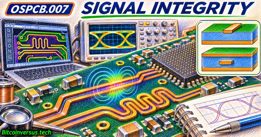
OSPCB.007 introduces PCB signal integrity: keeping digital voltage transitions recognizable after they travel through copper tracks. A high-speed trace behaves partly like a transmission line, not merely a wire connecting two pins. Its impedance, propagation delay, return path and proximity to other signals can produce reflections, timing errors or crosstalk. KiCad 10 provides tools for planning controlled routing, but passing design-rule checks does not prove that a high-speed interface will work.
Phil’s Lab, “PCB Controlled Impedance” (March 17, 2026), explains microstrip and stripline geometry and its role in high-speed digital design. Independent engineering instruction, not measurements of the training board. Credit: Phil’s Lab / YouTube.
Elementary overview and prerequisites
Imagine electrical signals as fast-moving waves rather than slowly flowing water. If a wave reaches a connector, via, termination or trace-width change whose impedance differs from the path, some energy can reflect toward the source. Fast rising edges matter even on a relatively low-frequency clock. Begin with PCB layers and stackups, return-current paths, and the OSPCB.006 decoupling lesson.
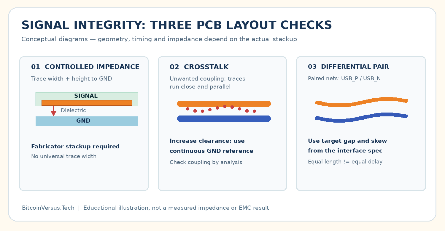
Three design decisions
- Controlled impedance: A trace’s copper width and thickness, dielectric properties, and distance to its reference plane affect characteristic impedance. A 50-ohm single-ended line is common in RF work, but not a universal target for every digital trace.
- Crosstalk: Changing current or voltage in a neighboring trace can couple energy into another. More spacing, shorter parallel runs and a nearby continuous reference plane can reduce coupling; no fixed spacing multiple guarantees compliance.
- Differential pairs: Paired nets such as
USB_PandUSB_Ncarry related signals. Maintain the interface-specific gap, impedance, reference continuity and permitted skew; treating every pair as a 100-ohm design is incorrect.
Worked example: trace length versus edge time
Assume a hypothetical transmission medium with an effective relative permittivity of 4. Its idealized signal velocity is approximately 300 / √4 = 150 millimeters per nanosecond. A 60 mm trace then has a one-way flight time of 0.40 ns. Compared with an assumed 0.50 ns signal rise time, that travel time is substantial. The result explains why reflections can matter even over a few centimeters; it does not predict a specific eye diagram, impedance or signal failure. Actual board velocity depends on the stackup and frequency.
Altium Academy, “The Easiest Ways to Reduce Crosstalk in a PCB” (May 18, 2023), discusses conductor spacing, reference-plane distance and simulation. Educational demonstration from an EDA vendor, not a measurement of the sample calculation. Credit: Altium Academy / YouTube.
KiCad 10 layout exercise
- Open a non-energized training PCB and identify the schematic nets requiring controlled impedance or matching.
- Enter the manufacturer-approved dielectric thicknesses and copper layers under Board Setup → Physical Stackup.
- Create a Tuning Profile containing the specified impedance, trace width and pair gap, then assign it to the appropriate net class.
- Name differential nets using supported matching suffixes, such as
USB_PandUSB_N; route the pair using KiCad’s differential router (6). - Use pair-length tuning (8) or skew tuning (9) only when the interface timing budget calls for it. For mixed routing layers, review KiCad’s delay-based tuning rather than assuming equal physical lengths give equal delays.
- Inspect return-path continuity and neighboring trace spacing. Run Inspect → Design Rules Checker and record unresolved impedance, signal-integrity and fabrication questions.
The workflow extends OSPCB.004 routing and DRC and OSPCB.002 vias and through-holes. A DRC pass confirms configured geometric checks, not actual impedance, eye opening or EMI performance. Fabrication stackup review, simulation and calibrated lab testing remain separate engineering steps.
Knowledge check and conclusion
Question: Why is a faster edge sometimes harder to route than a higher-frequency clock? Answer: Faster transitions contain high-frequency components that are sensitive to line discontinuities. Question: Does length matching guarantee timing matching? Answer: Not when layers, dielectric environments or transitions have different delays.
Successful high-speed PCB routing begins with a real stackup and an interface-specific electrical specification. Preserve the current-return route, reduce unneeded coupling and use KiCad’s tuning tools only against defensible targets.
Primary sources and calculations: KiCad 10 PCB Editor official documentation (physical stackup, tuning profiles, differential routing and time-domain tuning); Analog Devices, A Practical Guide to High-Speed PCB Layout; Altium technical article on PCB crosstalk; Phil’s Lab controlled-impedance lesson; Altium Academy crosstalk video. Example: 300 mm/ns ÷ √4 = 150 mm/ns; 60 mm ÷ 150 mm/ns = 0.40 ns. Material constant, trace length and rise time are chosen teaching assumptions, not measured properties of a circuit.
Editor’s Note: OSPCB.007 follows the published OSPCB.006 decoupling chapter. Source documentation supports the distinction among controlled impedance, coupling, timing skew and KiCad’s design checks. The propagation-delay example is an idealized arithmetic exercise, not a PCB simulation or tested timing limit. The 1200 × 630 colored-pencil cover contains only the lesson identifier, a two-word title and the small neon-green Bitcoinversus.tech watermark—far less explanatory text than the preceding cover. The in-story diagram is original and conceptual. The two videos have verified public titles, channels and watch identifiers; actual playback and mobile layout remain separate checks. No KiCad project was opened, board fabricated, network analyzer used or EMI compliance test performed.

BitcoinVersus.Tech is volunteer-run and publishes independent technical education. An optional 5,000-satoshi donation supports ongoing research. Scan the original QR from a second screen with a compatible Bitcoin wallet; on the same phone, use a wallet capable of reading a saved image if supported. Independently verify recipient address 3C9o19EH5HSiwEPyCTmEKzxhNCbo2X6TTb and amount before sending. Bitcoin transfers are generally irreversible.
We volunteer daily to ensure the information on the BitcoinVersus.Tech platform is Verifiably True. Coverage is educational and informational; it is not individualized electrical engineering certification, manufacturing approval, financial or investment advice.


Leave a Reply