
OSPCB.008 moves from circuit-board routing to the files a fabricator actually receives. The KiCad team released version 10.0.8 on October 30, 2026, correcting several board-editor and export issues, including ODB++ imperial copper-weight output. A PCB can look finished in the editor yet contain an open net, missing board edge or misidentified drill hole. Manufacturing handoff therefore requires more than clicking Export.
DigiKey, KiCad 9.0 Getting Started Part 6 — Laying Out Your First PCB (August 13, 2025). Official distributor tutorial covering stackup constraints, routing and DRC. The interface shown predates KiCad 10. Watch on YouTube.
Start with the fabricator’s limits
Review the layer stackup, board thickness, copper weight, drill sizes and spacing capability before release. A board drawn with a 0.20 mm clearance exceeds a hypothetical 0.15 mm minimum by 0.05 mm; neither value is a universal manufacturing requirement. The chosen fabricator’s approved specifications govern. Earlier routing and DRC and ground-return lessons explain common geometry problems.
Run DRC before plotting output
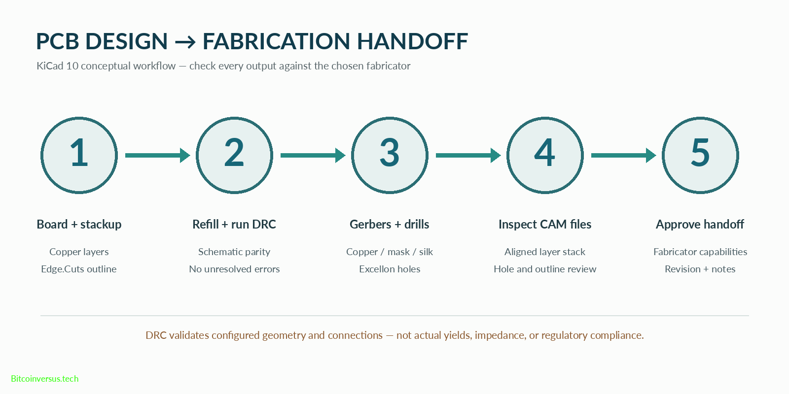
In KiCad’s PCB Editor, refill copper zones, then use Inspect → Design Rules Checker. Include schematic parity where applicable. Investigate unconnected pads, clearance errors, too-small holes, missing copper and ignored warnings. KiCad 10 also offers a graphical custom-rule editor. Record deliberate exceptions instead of suppressing errors to force a clean report. A passing DRC confirms configured rule checks; it cannot prove signal integrity, acceptable yield or compliance with EMC standards. The preceding OSPCB.007 signal-integrity lesson explains the remaining electrical risks.
Export the fabrication package, then inspect it
Use File → Fabrication Outputs → Gerbers to plot the required copper, solder-mask, silkscreen and Edge.Cuts layers. Generate drill files separately; most board houses accept Excellon, while KiCad also supports Gerber X2 drill outputs. Preserve a consistent drill origin and confirm that plated and nonplated holes are correctly identified. For assembly orders, include agreed solder-paste, placement and bill-of-materials files. Bare-board fabrication alone does not always need assembly data.
DigiKey, KiCad 9.0 Getting Started Part 7 — Images, Gerber Files and BOM (August 27, 2025). Official distributor video demonstrating DRC, Gerber plotting, drill generation and CAM review; archival training, not a KiCad 10.0.8 demonstration. Watch on YouTube.
Open the exported layers in KiCad’s Gerber Viewer, not merely the editable PCB layout. Check the outline, copper alignment, solder-mask openings, silkscreen clipping and drill hits. Compare the finished package with OSPCB.002 on plated holes and vias and OSPCB.006 on capacitor placement. KiCad can alternatively export IPC-2581 or ODB++, but only substitute a format when the manufacturer explicitly accepts it.
Record what was actually checked
A useful handoff includes the source project revision, Gerber/drill package, stackup and fabrication notes, chosen units, and a record of DRC findings. Do not infer finished-board quality from a screenshot of a green checkmark. Inspection, electrical test, controlled impedance and assembly inspection are distinct manufacturing or laboratory activities that may need additional orders and documentation.
Knowledge check
Question: Can a board pass DRC yet fail in production? Answer: Yes—electrical performance and manufacturing capabilities extend beyond configured layout rules. Question: Are Gerbers enough to communicate hole locations? Answer: Usually not; supply approved drill outputs too. Question: Does the latest patch change the fundamental handoff process? Answer: No; version 10.0.8 fixes defects but does not eliminate the need for independent CAM review.
Primary references: KiCad 10.0.8 PCB Editor manual (DRC, plotting, drill files, IPC-2581 and ODB++); KiCad 10.0.8 release notes, October 30, 2026; DigiKey’s verified August 2025 Part 6 and Part 7 video tutorials. The 0.05 mm margin is a labeled arithmetic example, not a measured tolerance or a manufacturing recommendation.
Editor’s Note: OSPCB.008 follows the published OSPCB.007 signal-integrity chapters. KiCad commands and output formats were checked against version 10.0.8 documentation and the dated release notes. The cover and step diagram are original illustrations with a single neon-green Bitcoinversus.tech credit. Both YouTube videos are identified archival tutorials; their playback must be checked separately. No PCB project, Gerber file, CAM job or manufactured board was tested during reporting.
BitcoinVersus.Tech is volunteer-run. Optional 5,000-satoshi donations support independent research. Scan the QR from a second screen using a compatible Bitcoin wallet; on the same phone, use an image-import feature if the wallet supports it. Confirm recipient 3C9o19EH5HSiwEPyCTmEKzxhNCbo2X6TTb and the amount before sending. Bitcoin payments are generally irreversible.
We volunteer daily to ensure information on the BitcoinVersus.Tech platform is Verifiably True. Coverage is educational and informational, not individual fabrication approval, electrical certification, financial or investment advice.


Leave a Reply