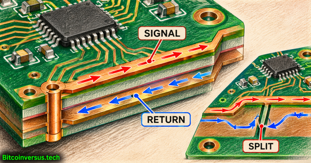
PCB ground planes and return-current paths determine how electrical signals complete their circuits after leaving a source. Routing a copper trace correctly is only half of the task: current must also return through a sufficiently continuous, low-impedance conductor. A copper zone can provide that return route, but gaps, slots, narrow necks and unexpected layer changes may increase loop area, coupling and electromagnetic interference even when a PCB design-rule check reports no geometric errors.
Elementary Overview
Electric current needs a complete loop, like water needing a path back to the pump. A printed circuit board carries current outward through one copper connection and back through another. Designers often spread a large sheet of copper across part of a board to give many circuits a shared return path, commonly called a ground plane.
For fast-changing signals, a return current generally stays near the outgoing trace when a continuous reference plane lies alongside it. A break in the reference copper can force a longer path. Earlier articles explain printed circuit board fundamentals, copper layers and stackups, and trace routing and clearances. The next skill is checking where current actually returns, not simply where the visible signal trace goes.
Altium Academy, “Return Path Basics for Mixed Signal PCB Design” (March 27, 2026), presented by Zach Peterson. Official EDA-vendor education on displacement current and why reference-plane continuity matters; not a measurement of the sample board discussed below.
Learning Objectives and Prerequisites
- Differentiate a copper zone outline, filled copper, net assignment and a genuine continuous return path.
- Explain why fast return currents tend to cluster near the signal route while steady DC return follows the resistance distribution.
- Inspect KiCad 10 zone properties, thermal reliefs, priorities and isolated copper islands.
- Recognize plane slots, gaps and layer transitions that require further signal-integrity review.
- Distinguish DRC connectivity checks from electrical simulation, laboratory validation and manufacturing approval.
Prerequisites: basic circuit current, resistance, a PCB schematic with a GND net, and familiarity with vias and plated holes. Examples are educational, not finished manufacturing or safety-critical PCB designs. A particular board stackup, copper weight, material and intended signal spectrum must be confirmed before hardware release.
Return Current Is Part of the Signal Loop
Every complete current path includes an outbound portion and a return portion. At low frequencies or steady DC, copper resistance has a strong influence on current distribution. At higher frequencies, impedance includes the effects of inductance and capacitance, so return current tends to follow nearby reference copper that minimizes loop inductance. The return is distributed through conductive material rather than flowing as a single perfect line.
Analog Devices explains that a solid plane directly beneath a signal trace reduces loop area and magnetic-field coupling, while a split plane forces some current around the interruption. The underlying principle appears in ADI’s PCB layout and return-current discussion and its mixed-signal grounding analysis. The word ground does not imply zero voltage everywhere: physical copper has resistance, inductance and finite current-carrying ability.
A copper fill placed on the same layer as signal routing may be fragmented by tracks and pads. A dedicated neighboring copper plane can offer more reliable reference continuity, but merely adding green-colored fill in an editor does not prove that any high-frequency trace has a good return path.
Continuous Ground Plane Versus a Split Plane
Imagine a signal crossing a narrow void in the reference plane. The signal conductor can remain perfectly connected and pass spacing rules. The nearby return current, however, cannot cross the missing reference copper and may detour around the end of the slot or seek another permitted path. Depending on the current’s frequency content, the longer loop can increase radiated emissions, crosstalk or waveform disturbance.
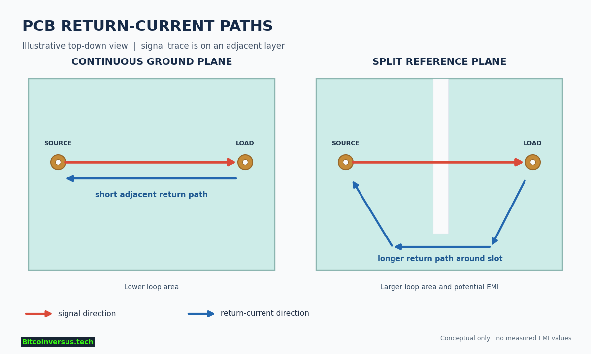
Analog Devices recommends keeping sensitive traces above uninterrupted reference copper wherever practicable. Routing a high-speed trace across an isolation gap can be a design problem even if KiCad reports the net electrically connected. The appropriate correction may be moving the trace, relocating the split or reconsidering the stackup; adding an arbitrary bridge is not a universal repair.
Why KiCad Copper Zones Need Both Net Assignment and Refill
KiCad 10’s PCB Editor manual describes zones as filled or hatched copper regions assigned to a net. Their polygon outlines establish where copper may be generated; the outline itself is not fabricated metal. A GND zone normally keeps configured clearance from objects on other nets, clips to the board boundary and may use solid or thermal-relief connections to pads.
In the PCB Editor, use the Add Filled Zone tool or the documented default shortcut Ctrl+Shift+Z. Choose the relevant copper layer and the GND net, then define the zone outline. After placing or modifying routed objects, refill zones with the documented default B shortcut. KiCad’s zone fill is not automatically recalculated after every edit by default, although automatic refill can be enabled in preferences. Always refill before final DRC and manufacturing exports.
A GND-labeled polygon should never be presumed electrically useful merely because its outline covers the board. The resulting filled copper can be broken into sections by keepouts, cutouts and clearances. Designers should inspect the finished filled geometry on every relevant layer and confirm the expected copper is attached to the correct nets.
Thermal Reliefs, Islands and Copper Neckdowns
A thermal relief connects a pad to a surrounding copper zone using narrow spokes instead of covering the entire pad perimeter with solid copper. The spokes reduce heat sinking during soldering, but they also add a localized current path whose width and count must suit the actual application. High-current pads may require different, manufacturer-reviewed connections; a solder-friendly relief is not necessarily suitable for every power connection.
KiCad 10 can remove isolated filled-copper islands and includes parameters for minimum filled width, clearances, thermal relief gaps and spoke widths. Its zone manager controls priorities where zone areas compete for space. An isolated copper patch may behave like floating metal rather than an intentional ground connection; a very narrow neck may create unwanted impedance even when basic connectivity exists. Footprints and pad geometry also influence whether a zone can connect as intended.
No single clearance, spoke or stitching-via dimension is appropriate for every fabrication process or signal speed. Obtain fabrication capability limits from the board house and electrical performance requirements from the circuit design, not a generic screen capture.
Reference Changes and Ground Stitching Vias
When a signal changes from one copper layer to another using a via, its nearby reference environment can change as well. Connecting same-net ground regions with appropriately located GND stitching vias may help provide a return-current transition when the relevant planes are physically connected. A decorative via disconnected from the necessary copper does not solve the problem. A return transition between different reference nets can involve a more complicated power-distribution and decoupling design.
The correct via count, spacing, isolation and capacitor placement depend on layer geometry, frequency spectrum and component guidance. Blindly placing many ground vias cannot guarantee impedance control or electromagnetic compatibility. Review the pads and vias lesson before making such changes, and confirm manufacturability with the chosen fabricator.
Authentic PCB Hardware and Physical Copper
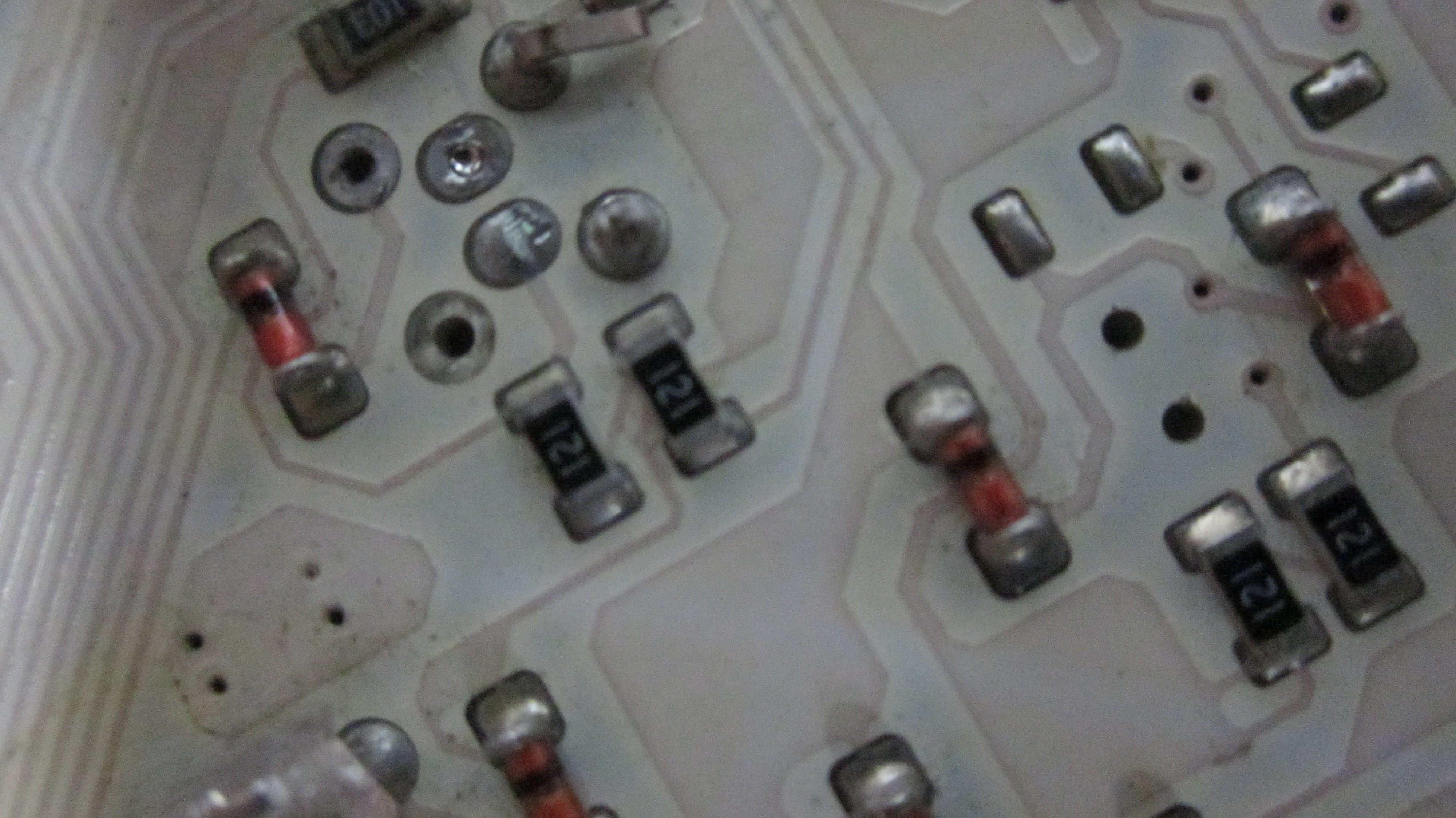
A finished board’s traces, plated holes, solder mask and components are physical objects. The image below illustrates patterned copper on manufactured hardware, not the current distribution inside a reference plane. Internal planes may not be visible in an ordinary photograph.
Ampnics, “How to use cupper filled zone in KiCAD | Part 14 | KiCAD 9.0” (March 28, 2025). Independent step-by-step demonstration of zone net assignments, copper pours and thermal reliefs; precise KiCad 10 settings are governed by the current version’s official manual.
Illustrative Loop-Area Calculation
Consider a simplified rectangular loop model with 40 mm of signal length and a 0.2 mm separation between the signal trace and its adjacent reference. The nominal geometric area is 40 mm × 0.2 mm = 8 mm². If a hypothetical reference-plane interruption forced the average return path to sit 5 mm away for the same 40 mm span, the simplified area would be 40 mm × 5 mm = 200 mm², a factor of 25 larger.
The calculation demonstrates how separation changes a toy loop-area estimate; the full field is distributed and real PCB electromagnetic behavior is not represented by a single rectangular path. An area ratio alone cannot predict emissions, timing error or impedance. A production design may need field simulation, validated layout rules and laboratory EMC testing.
KiCad Verification Workflow
- Start from a netlist with confirmed schematic ground connections and an approved copper stackup.
- Assign each intended copper zone to the correct net and verify the chosen layers, minimum widths, keepouts, thermal connections and priorities.
- Refill all copper zones, then inspect the actual fill rather than relying on the polygon outlines.
- Use KiCad DRC to check documented clearance, connectivity and relevant geometric errors; investigate warnings rather than suppressing them blindly.
- Visually trace the nearby return path for fast signals across layer changes and near plane cutouts, noting any discontinuities DRC cannot interpret as a signal-integrity risk.
- Review final fabrication outputs and validate the design against device datasheets, board-fabrication limits and the required electrical testing plan.
KiCad’s Getting Started documentation describes filling copper zones, observing thermal spokes and checking rules. Passing DRC is necessary in many workflows but not sufficient evidence of signal integrity, appropriate current capacity, controlled impedance or manufacturing readiness.
Troubleshooting Common Zone Problems
- Ground pad appears disconnected: inspect net assignment, pad stack, thermal gap, spoke width and zone refill state.
- Zone breaks into islands: check tracks, keepouts, board cutouts, minimum width, island removal settings and actual net continuity.
- Fast signal crosses a plane slot: reroute it over continuous reference copper where feasible; document an engineered alternate return scheme if unavoidable.
- Mixed-signal noise persists: review component placement and return-current partitioning before splitting ground indiscriminately. Analog Devices’ mixed-signal layout guide explains why one continuous plane is often preferable for simpler mixed-signal designs.
- DRC passes but EMI testing fails: examine the real loop geometry, switching transitions, cables, shielding, and reference changes. DRC does not substitute for electromagnetic analysis or test.
Knowledge Check With Explanations
- Is a zone outline manufactured copper? No; the filled geometry is the intended copper output.
- Does GND net assignment guarantee a continuous high-frequency return path? No; a zone may have slots, islands or neckdowns.
- Why may a high-speed return current run close to the outbound trace? The nearby path commonly reduces loop inductance and overall impedance.
- What purpose do thermal spokes serve? They help solderability by limiting heat transfer to a large copper plane, subject to current requirements.
- What does the KiCad default B shortcut do? Refill all zones in the PCB Editor.
- Does a clean DRC prove EMC compliance? No; geometric rules and electromagnetic behavior are different checks.
Primary References
Primary references: KiCad 10 PCB Editor Manual — Working with Zones; KiCad 10 Getting Started — Copper Zones and DRC; Analog Devices — Avoid PC-Layout Gotchas in ISM-RF Products; Analog Devices — Successful PCB Grounding with Mixed-Signal Chips; and Analog Devices — Basic Layout Guidelines for Mixed-Signal PCBs. The video links supply additional instruction, and manufacturer-specific layout guidance takes precedence over simplified illustrations.
Elementary Conclusion
A printed circuit board needs a way for electricity to return after travelling along a trace. A wide copper ground plane can give that returning current a nearby route, especially for quickly changing signals. If a gap blocks the route, current may take a longer path and interfere with other parts of the board. Correct PCB design checks the copper fill, the entire current loop and the physical board requirements instead of trusting the signal trace alone.
Editor’s Note: Internal Open Source TechCert PCB curriculum slot OSPCB.005 follows published OSPCB.004. Technical statements were checked against KiCad 10 and Analog Devices source documentation. The loop-area numbers are transparent hypothetical calculations, not an impedance simulation, measured current distribution or certified board geometry. The 1200 × 630 branded cover is original colored-pencil conceptual artwork; the instructional return-path diagram is original and not a field solver. The physical PCB photograph is genuine CC0 media with attribution. The YouTube sources were identified by video title, channel and public listing; actual playback and public mobile-view verification are separate checks. No EDA project was opened, no Gerber was exported and no PCB was fabricated or measured.

For mobile scanning, display the donation QR on a separate screen and scan it with a compatible Bitcoin wallet. On the same phone, some wallets support reading an image saved from the page. Verify the recipient before donating 5,000 sats: 3C9o19EH5HSiwEPyCTmEKzxhNCbo2X6TTb.
We volunteer daily to ensure the credibility of the information on this platform is Verifiably True. If you would like to support our work and help further secure the integrity of our research initiatives, please scan the original QR code above to donate 5,000 sats.
BitcoinVersus.tech is not a financial advisor. This media platform reports on financial subjects purely for informational purposes.


