MemryX AI has announced a new accelerator architecture aimed at taking compact inference hardware beyond one peta-operation per second without moving every deployment into a high-power GPU server. The Michigan semiconductor developer unveiled MX3+ on November 10, 2026, setting a target of more than 1 POPS and 2.16 GB of distributed on-chip memory across a 16-chip configuration. Both figures are design goals, not independently benchmarked shipping results.
The company expects engineering samples in late 2027 and volume production around mid-2028. Its existing MX3 processor is commercially available; MX3+ remains in development. Rather than another announced mass-production milestone, the news is a roadmap commitment for AI-equipped cameras, robots, factories and edge servers requiring larger models without a major power or cooling increase.
MemryX’s official demonstration of 100 streaming videos on four MX3 modules, published May 2025. Footage demonstrates the available MX3 platform, not the future MX3+. Credit: MemryX/YouTube.
Ten times the compute, nearly ten times the memory
According to MemryX’s original announcement, the successor targets up to ten times MX3’s peak compute and nearly ten times its on-chip memory while remaining within the same low-power operating envelope. The company also aims to maintain the predecessor’s compact footprint and software development workflow. Its 16-chip proposal would work as one logical accelerator, with the Neural Compiler distributing models among chips.
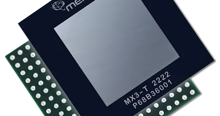
For reference, the current MX3 product specification lists 6.25 TFLOPS, 10.5 MB of on-chip weight memory and roughly 0.2–3 W per chip. MX3 uses a near-memory dataflow design intended to move model weights and intermediate results less often between memory and processing units. MX3+ is intended to accommodate larger convolutional networks, transformers, small language models and vision-language-action workloads without switching architecture.
One POPS is not automatically one PFLOPS
A peta-operation means one quadrillion operations, but the announced POPS figure lacks a published precision and workload definition. Floating-point operations, integer operations, theoretical peak arithmetic and real application throughput cannot be treated as interchangeable measures. Likewise, 2.16 GB is the projected aggregate distributed on-chip memory for 16 accelerators, not necessarily a single contiguous pool available to every model.
The distinction matters when comparing emerging AI hardware. Axelera’s Titania targets much larger air-cooled installations, while the DEEPX DX-M2 emphasizes low-wattage embedded inference. Neither competing target constitutes an apples-to-apples benchmark against MX3+ without common precision, model mix and measured wall power.
Cadence Design Systems explains MemryX’s earlier MX3 architecture, silicon-design workflow and low-power edge inference in a March 2025 engineering video. Credit: Cadence/YouTube. The video predates MX3+.
Why greater on-chip memory could matter
An edge accelerator that can keep more weights close to computation may reduce trips to external DRAM and allow deeper inference pipelines. That can improve latency consistency where cameras must trigger a sorting actuator or an autonomous robot has to respond rapidly. But performance still depends on data formats, compiler mapping, model accuracy, memory capacity, chip-to-chip traffic and host-system overhead. An announced peak rating alone cannot establish an application-level advantage.
The architecture remains distinct from the memory-expansion approach reported in Penguin Solutions’ 1 TB CXL card, where external memory capacity is the central feature. MemryX aims to increase on-chip availability instead. The broader inference ecosystem, including the new SGLang consortium, illustrates why hardware speed must be considered alongside scheduling and software efficiency.
Prospective buyers still lack independently measured tokens per second, frames per second, sustained power, supported model sizes, pricing and production yields for MX3+. Until silicon is sampled, the credible conclusion is a potentially important architectural target with a roughly two-year route to volume manufacturing, rather than a validated 2026 performance breakthrough.
Sources and verification
Primary documentation: MemryX press announcement, November 10, 2026; MX3+ roadmap and product description; shipping MX3 technical specifications; original distributed release; official MemryX demo and Cadence technical video. Peak targets and schedules are attributed to MemryX; no MX3+ measurements are represented as laboratory-confirmed results.
Editor’s Note: The November 10 announcement is confirmed, but MX3+ remains in design. Targets above 1 POPS, 2.16 GB distributed memory, tenfold compute and the 2027–2028 schedule are supplier projections. The original photorealistic 1200 × 630 featured cover depicts a conceptual semiconductor inspection, not MemryX’s actual hardware or personnel. The in-story authentic photograph shows the existing MX3 chip, and the two verified-source videos demonstrate its predecessor technology, not MX3+ engineering samples. Successful playback and mobile responsiveness require independent browser checks.
Support BitcoinVersus.Tech
Optional contributions of 5,000 satoshis help support independent research and reporting. Scan the original BitcoinVersus.Tech donation QR using a compatible Bitcoin wallet on a second device. On mobile, save the QR image and import it with a wallet supporting image-based QR scanning, if available. Verify the recipient and payment amount before authorizing a transaction.

BitcoinVersus.Tech is volunteer-run and publishes independent research and technical journalism. Optional donations support continued coverage; no contribution is required. Confirm Bitcoin recipient 3C9o19EH5HSiwEPyCTmEKzxhNCbo2X6TTb and 5,000 satoshis before paying. Bitcoin transactions can be irreversible. Product-performance claims and forecasts are informational, not procurement or investment advice.


Leave a Reply