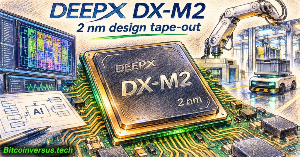
South Korean semiconductor designer DEEPX has completed the design tape-out of its DX-M2 artificial intelligence processor, advancing a planned Samsung Foundry 2-nanometer chip for robots, industrial machines and other devices that need local generative-AI inference. The design targets approximately 5 watts for the processor itself and 80 trillion operations per second (TOPS), but first silicon is not expected until March 2027. Tape-out is an engineering milestone, not a proven production-chip benchmark.
DEEPX confirmed the November milestone in statements reported by EE Times and Yonhap. Manufacturing is planned on Samsung’s second-generation 2 nm SF2P process. The CES 2027 Innovation Awards listing independently confirms honoree status, not achieved silicon performance.

What the design actually promises
The manufacturer’s published specifications describe an 80 TOPS neural processing unit, up to 96 GB of externally attached LPDDR5X memory and 153.6 GB/s peak memory bandwidth. The expected performance class differs from ordinary image-recognition accelerators: DEEPX wants its chip to serve large language models and vision-language models directly inside equipment, limiting dependence on remote GPUs and network connections.
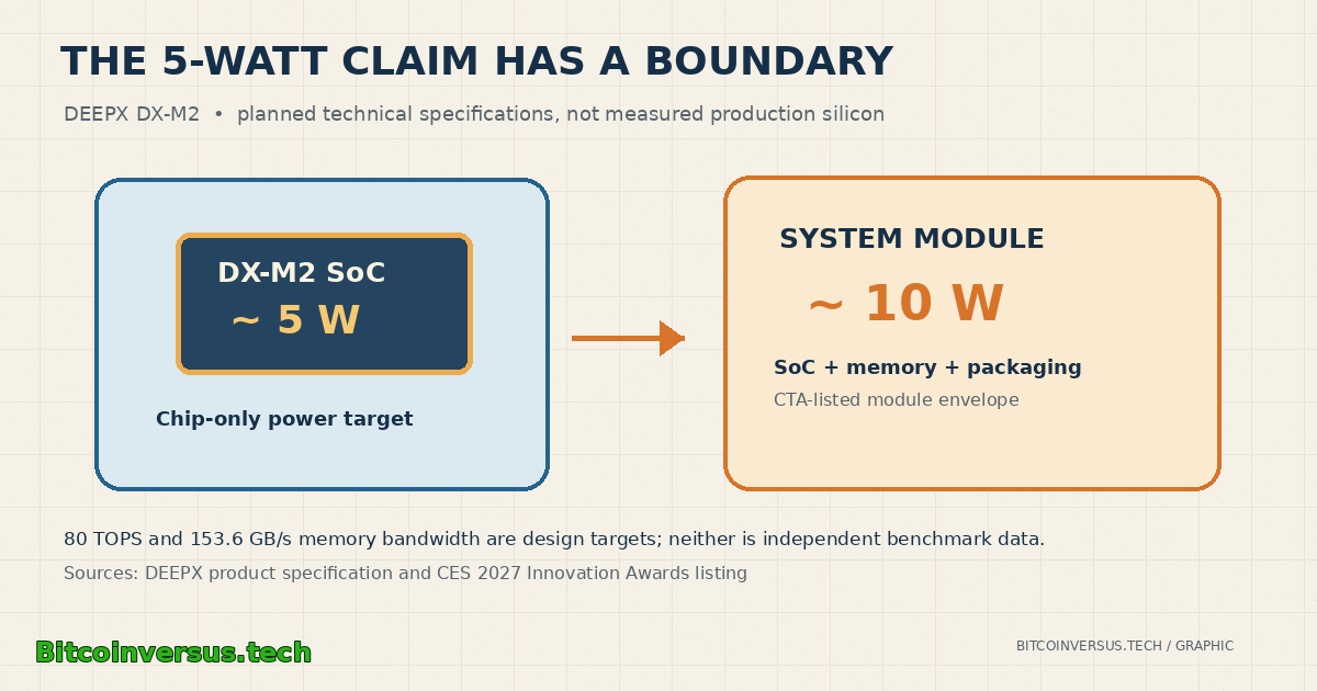
Power figures require careful separation. DEEPX lists 5 W for the DX-M2 system-on-chip alone, while the CES product description specifies an approximately 10 W complete module envelope. Memory and supporting electronics consume additional electricity. A 5 W chip claim cannot automatically be applied to an entire robot, AI computer or memory-equipped board. For background, BitcoinVersus.Tech explains the different jobs handled by CPUs, GPUs and NPUs.
Why memory may matter more than TOPS
Inference workloads often move model weights between DRAM and computational units repeatedly. DEEPX told EE Times that it tripled bandwidth from about 50 GB/s on its earlier design to a stated 150-plus GB/s on DX-M2. Samsung processor-in-memory technology is also being evaluated to reduce data movement, although its potential speedups are simulation results and may require additional power. Our high-bandwidth memory explainer covers the broader relationship between AI accelerators and memory systems.
Model capacity also needs context. A 100-billion-parameter model stored at four bits per parameter requires roughly 50 GB for weights alone, before caches, activations, software and metadata. DEEPX forecasts roughly 10–30 generated tokens per second for certain 20B–100B-parameter models, with active parameter counts potentially much smaller in mixture-of-experts designs. No independent DX-M2 silicon benchmarks were available at publication.
An official DEEPX newsroom link to the company’s November 6 demonstration of 64-channel video surveillance and vision-language AI. The video concerns the broader existing edge-AI platform; it is not a DX-M2 post-silicon test. Credit: DEEPX / YouTube.
First samples are still months away
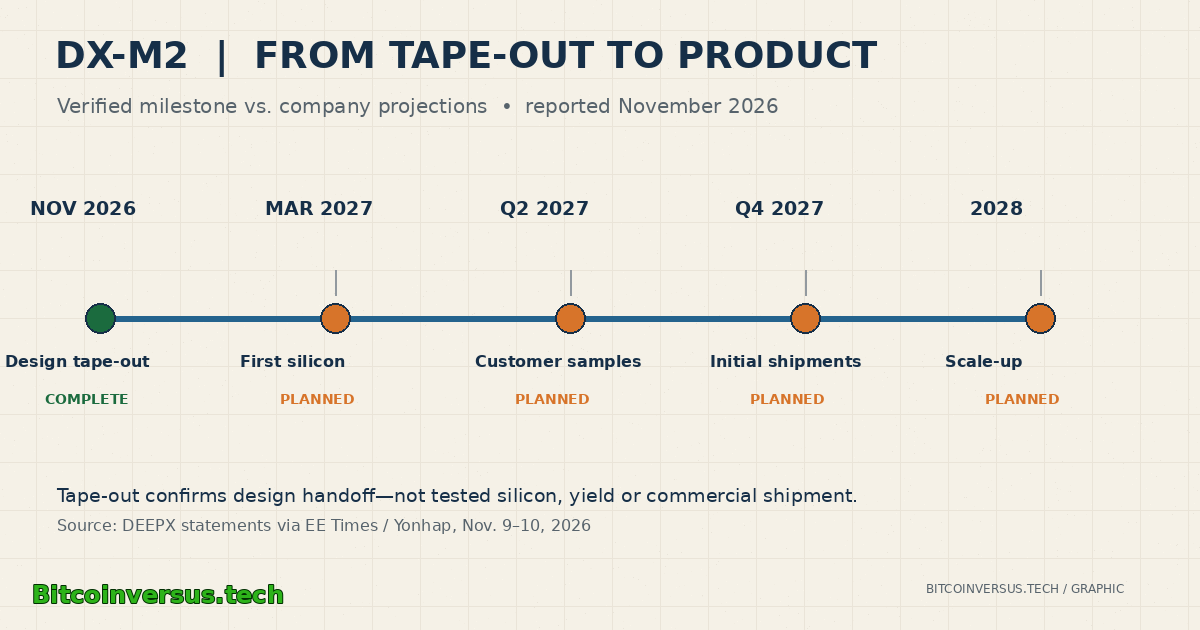
The production schedule remains a series of targets: first silicon in March 2027, customer evaluation samples in the second quarter, initial production shipments in the fourth quarter and wider production in 2028. Silicon bring-up, yield, memory integration, thermal testing and real workload compatibility could all change the timetable. DEEPX has shipped its earlier DX-M1 product, but that history does not establish DX-M2 production readiness.
A successful launch would give robotics developers another option for running inference near sensors and actuators, potentially improving privacy, latency and intermittent-network operation. BitcoinVersus.Tech has also covered BrainChip’s development hardware and STMicroelectronics’ industrial chip roadmap, illustrating how diverse low-power computing requirements have become.
The principal unknowns are real chip yield, repeatable model throughput, complete system power, pricing and developer-tool maturity. DEEPX’s tape-out gives Samsung a prospective advanced-node customer, but it does not yet prove a commercial advantage against other semiconductor foundries or established accelerators. BitcoinVersus.Tech previously examined the challenges facing foundries seeking third-party manufacturing customers.
Sources and verification: DEEPX DX-M2 product specification, CES Innovation Awards honoree listing, EE Times interview and technical assessment (November 9), Yonhap company statement (November 10), The Elec process and schedule report (November 13). Forecast power, performance and production dates remain company-supplied claims.
Editor’s Note: DX-M2 design tape-out is reported as completed; a manufactured and independently benchmarked DX-M2 chip was not available for editorial testing. The 5 W processor target differs from the approximately 10 W module envelope. The 1200 × 630 colored-pencil cover is original conceptual artwork, not a genuine photograph of shipped silicon. The in-story DEEPX render is company-supplied, and the two engineering graphics are original and sourced. The official DEEPX YouTube link identifies an earlier technology demonstration rather than a DX-M2 performance test; live playback and mobile rendering have not been independently verified.

BitcoinVersus.Tech is volunteer-run and publishes independent educational technology reporting. An optional 5,000-satoshi donation supports ongoing research. Scan the original QR from a second screen with a compatible Bitcoin wallet; on mobile, use a wallet that supports scanning a saved image. Independently verify the recipient address 3C9o19EH5HSiwEPyCTmEKzxhNCbo2X6TTb and the payment amount before sending. Bitcoin transfers are generally irreversible.
We volunteer daily to ensure information on the BitcoinVersus.Tech platform is Verifiably True. Coverage is educational and informational and does not constitute financial or investment advice.


Leave a Reply