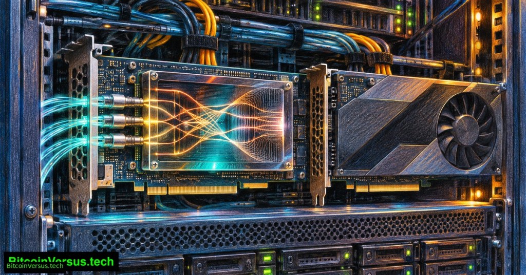
A new optical accelerator is taking over one of the mathematical jobs normally performed by electronic processors. On November 17, German computing company Q.ANT announced its NPU Gen 2+ at the SC26 supercomputing conference in Chicago. The company demonstrated a hybrid arrangement combining its photonic processor with an AMD GPU to run a large language model, moving a Fourier-based computation into light.
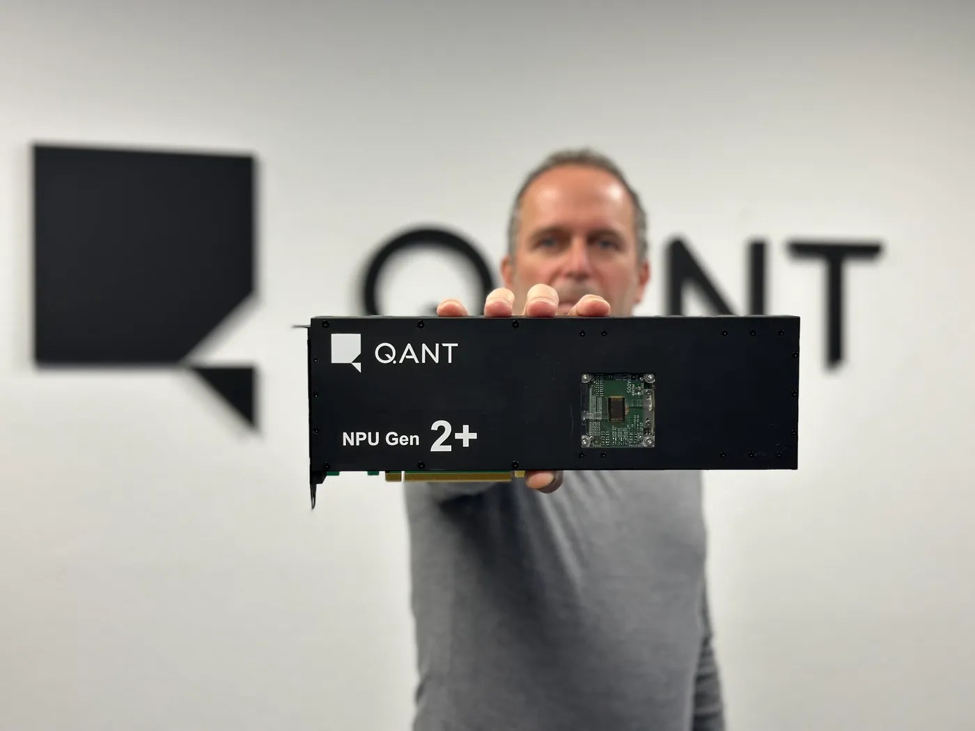
What the photonic processor actually does
The new operation is a discrete Fourier transform (DFT), a mathematical technique that converts a sequence into its frequency components. Fourier transforms help process signals and images and can support alternative neural-network architectures. Rather than executing every transform through long chains of digital arithmetic, Q.ANT uses a specially designed optical component to carry out the operation through the behavior of light.
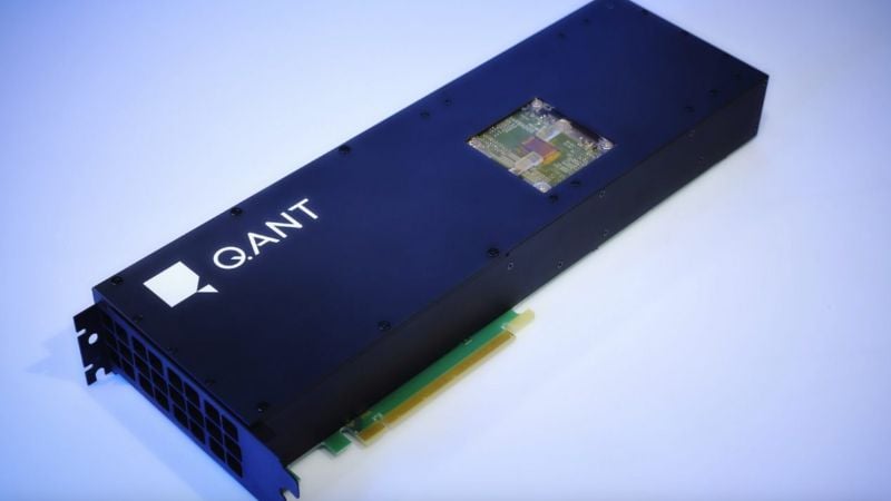
According to Q.ANT’s product description, Gen 2+ has 16 optical cores, compared with eight on Gen 2. Its thin-film lithium-niobate photonic circuitry is intended to work alongside conventional computing, not replace general-purpose CPUs, GPU memory, storage or networking. A rack-mountable server design and PCIe integration make the concept relevant to data-center operators exploring heterogeneous accelerators.
At SC26, Q.ANT reported substituting an optical Fourier-based operation for an expensive component of a language-model attention pathway. The important qualification is experimental scope: the announcement establishes a demonstration of a hybrid language-model workload, not a broadly validated improvement across all contemporary models.
Why a hybrid architecture matters
Most AI installations are built around electronic accelerators because they support programmable arithmetic, large memory systems and mature software frameworks. Optical processing can be efficient for selected mathematical functions, but conversion between electronic and optical signals, data movement, numerical precision and model compatibility still affect system-level performance. A chip-level speed advantage cannot automatically be extrapolated into a lower electricity bill for an entire rack.
Those practical constraints align with a larger industry interest in photonics. Penguin Solutions and Marvell are pursuing optical memory connectivity, while MIT researchers are investigating alternative electronic device structures. The projects address different bottlenecks and should not be measured as interchangeable solutions.
Software access and the commercial timeline
Q.ANT released a developer toolkit in September with C and Python interfaces, examples and a CPU-based simulator. Its latest announcement says support for the new Fourier operations is being extended. Developers can explore photonic-friendly algorithms before committing to hardware, building on the company’s earlier open SDK announcement.
The company targets commercial systems combining Gen 2 and Gen 2+ in the second half of 2027. Until independent tests disclose end-to-end model accuracy, throughput, power draw and cost under comparable workloads, higher performance and energy efficiency remain possibilities rather than verified general-purpose outcomes. Similar engineering tradeoffs appear in battery-manufacturing process improvements, where a faster individual step does not settle the complete system economics.
Sources and verification
- Q.ANT announcement, November 17, 2026
- Q.ANT product specifications and proof-of-concept status
- Data Center Dynamics coverage, November 19, 2026
- Q.ANT official Gen 2+ image and All About Circuits earlier-generation hardware photo
Editor’s Note: Q.ANT’s product and demonstration statements are attributed to the company. No independently measured, standardized Gen 2+ versus GPU efficiency result was identified in the reviewed sources. Cover is conceptual colored-pencil illustration, not an actual photograph of the processor. In-story photographs depict Gen 2+ and an explicitly labeled earlier NPU 2, respectively; none documents the SC26 live demo.
Editor’s Note: We volunteer daily to ensure the credibility of the information on this platform is Verifiably True. If you would like to support to help further secure the integrity of our research initiatives, please scan the QR code below

BitcoinVersus.Tech publishes journalism for informational purposes. Product demonstrations and company claims should not be treated as independent benchmarks or purchasing advice.


Leave a Reply