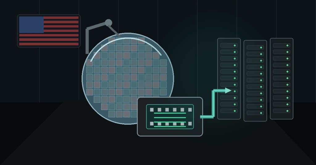
Navitas Semiconductor has moved its fifth-generation GaNFast power technology into U.S. manufacturing through GlobalFoundries, putting a new domestic source of gallium nitride power devices directly into the AI infrastructure supply chain.
On September 1, the companies said first shipments of U.S.-manufactured Gen 5 GaNFast technology would begin in September from GlobalFoundries’ 200 mm GaN-on-silicon manufacturing platform in Burlington, Vermont. The first family is expected to include 650 V GaN FETs spanning 11 mΩ, 18 mΩ, 50 mΩ, 120 mΩ and 150 mΩ on-resistance options.
A manufacturing milestone, not yet a full production ramp
The distinction matters. The September milestone is the start of wafer shipments, followed by internal samples expected in October and strategic-customer samples before the end of 2026. Independent semiconductor coverage notes that Navitas has not yet announced completed customer qualification, general availability or the start of high-volume production.
That still makes the move more concrete than a foundry agreement on paper. Navitas has adapted its proprietary Gen 5 device architectures to GlobalFoundries’ U.S. 200 mm GaN-on-silicon process, giving the company a domestic manufacturing path for power semiconductors aimed at AI data centers, high-performance computing, industrial electrification and national-security systems.
The same high-power pivot is showing up elsewhere in Navitas’ roadmap. BitcoinVersus recently covered the company’s U.S. Army program for 10 kV silicon-carbide devices, another example of its move away from lower-power consumer applications and toward infrastructure-scale power electronics.
A September 1 X post tracking the manufacturing announcement highlighted the Vermont fab, September wafer schedule and customer-sampling timeline while also pointing to the larger issue: AI infrastructure requires more than accelerators. It requires increasingly dense and efficient power conversion around them.
Why GaN matters to the AI power stack
Gallium nitride is attractive in high-frequency power conversion because it can switch faster than conventional silicon while supporting smaller magnetics and higher power density. In AI racks, those characteristics become more important as power distribution moves toward higher voltages and conversion stages are pushed closer to GPUs, CPUs and other accelerators.
Navitas has been positioning GaN alongside high-voltage silicon carbide as a grid-to-processor portfolio. The company uses SiC for higher-voltage stages and GaN for dense conversion closer to the rack and compute tray. A second verified X discussion laid out that architecture and the industry’s shift toward 800 V DC power delivery.
The broader U.S. semiconductor buildout is also moving beyond compute silicon. BitcoinVersus has tracked GlobalFoundries and Marvell expanding U.S. capacity for AI networking chips, showing how domestic infrastructure investment is spreading across networking, power and other supporting silicon rather than focusing only on GPUs.
Power density is becoming a semiconductor problem
AI infrastructure increasingly treats power delivery and thermal management as part of the compute platform. Faster switching and higher-density converters can reduce the physical size of power stages, but that does not eliminate the need to validate efficiency, reliability and thermals under sustained data-center loads.
That is why the GlobalFoundries transition is significant but should not be overstated. Manufacturing a 200 mm wafer in Vermont is one milestone. Customer qualification, packaged-device performance, reliability data and production availability are the next ones that determine whether Gen 5 becomes a meaningful part of future AI rack deployments.
The manufacturing story also sits beside a wider move toward larger-diameter wide-bandgap production. BitcoinVersus recently reported on Wolfspeed’s premium 200 mm silicon-carbide wafers, reinforcing how power-semiconductor scale and supply are becoming strategic pieces of the AI infrastructure buildout.
For Navitas and GlobalFoundries, the next test is execution: turning September wafer starts into qualified devices that can ship at scale. If that happens, U.S.-made GaN could become a more visible layer in the power architecture underneath the next generation of AI systems.
BitcoinVersus.Tech
Advertisement
Editor’s Note:
We volunteer daily to ensure the credibility of the information on this platform is Verifiably True. If you would like to support our research initiatives, please donate here: 3C9o19EH5HSiwEPyCTmEKzxhNCbo2X6TTb
BitcoinVersus.tech is not a financial advisor. This media platform reports on financial subjects purely for informational purposes.


Leave a Reply