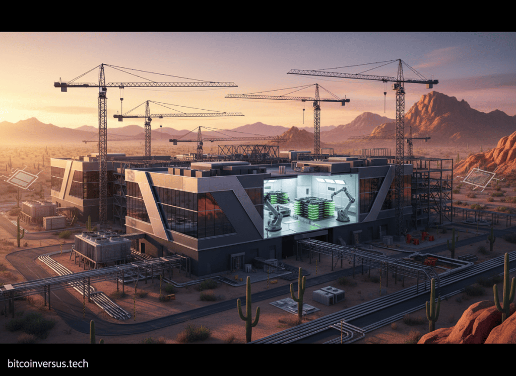
Amkor Technology is expanding its planned Arizona semiconductor packaging and test campus investment to about ₿143,800 ($12 billion), turning Peoria into one of the largest U.S. bets on the back end of the AI chip supply chain.
Using an October 1 reference of 1 BTC (about $83,448), the expanded project value is roughly ₿143,800 ($12 billion). Amkor disclosed the increase in a September 8 post, saying Phase 2 will significantly expand advanced packaging capacity in the United States.
In its official Phase 2 announcement, Amkor said strong customer commitments had already exceeded the 33,000 square meters of cleanroom capacity planned for Phase 1. Phase 2 is expected to add another 60,000 square meters, bringing the campus to roughly 93,000 square meters of cleanroom space.
Advanced packaging is becoming part of the AI compute bottleneck
Leading-edge wafers are only one part of an AI accelerator. High-performance processors increasingly depend on advanced packaging to connect compute dies, high-bandwidth memory, interposers and high-speed interfaces into one usable module.
That is why packaging capacity is becoming strategically important. A cutting-edge logic die cannot become a complete accelerator if the industry lacks enough packaging, bumping, assembly and test capacity to combine it with memory and validate the finished device.
BitcoinVersus.tech recently examined the same constraint in CoWoS-L’s push beyond traditional reticle limits, where packaging architecture becomes part of the performance roadmap rather than a final manufacturing step.
Phase 2 nearly triples planned cleanroom capacity
Phase 1 was planned around 33,000 square meters of cleanroom space. The newly announced Phase 2 adds 60,000 square meters, bringing the campus to about 93,000 square meters—roughly one million square feet of cleanroom capacity.
Amkor says the site will include wafer bump, probe, assembly and test capabilities. Those are the manufacturing steps that turn processed wafers into packaged semiconductor devices ready for server boards, accelerators, networking equipment, automotive systems and other end products.
InBusiness Phoenix’s coverage notes that the added Phase 2 cleanroom footprint nearly triples the originally planned capacity and pushes the Arizona project well beyond its earlier scale.
Arizona is becoming a full semiconductor cluster
The project matters because Arizona is no longer being built around wafer fabrication alone. TSMC’s manufacturing footprint gives the state front-end chip production, while Amkor adds outsourced packaging and test capacity close to those fabs.
BitcoinVersus.tech previously covered TSMC’s advanced packaging expansion, showing that the packaging bottleneck is being addressed on multiple fronts as AI chips become larger, more modular and more dependent on high-bandwidth memory.
Locating fabrication, packaging and test capacity in the same regional ecosystem can reduce logistics complexity and shorten the physical distance between wafer output and completed semiconductor modules.
Packaging and test hardware becomes more valuable as chips get more complex
Modern AI accelerators increasingly use chiplets, stacked memory and multi-die architectures. That shifts more performance risk into packaging and test because the finished module has more interfaces, more memory channels and more high-speed connections that must work together.
Testing therefore becomes part of the scaling challenge too. BitcoinVersus.tech recently covered Teradyne’s Magnum E2 platform for next-generation AI memory testing, another example of semiconductor infrastructure expanding around the complexity of AI hardware rather than only around transistor fabrication.
The workforce grows with the physical footprint
Amkor says Phase 1 and Phase 2 together are expected to support more than 3,500 Arizona-based employees. That workforce will sit inside a manufacturing environment that combines cleanroom operations, semiconductor process equipment, automated material handling, metrology, test systems and facility infrastructure.
Phase 2 construction is expected to begin in late 2027, with completion targeted by the end of 2029. That timeline means the project is a long-horizon capacity build rather than an immediate supply release.
The bigger story is where the AI supply chain is spending money
AI infrastructure spending is often discussed in terms of GPUs, accelerators and data centers. Amkor’s expansion shows another layer absorbing capital: the factories that package and test those chips before they ever reach a server rack.
At roughly ₿143,800 ($12 billion), the planned Arizona project is large enough to show that advanced packaging is no longer a secondary manufacturing step. It is becoming one of the core infrastructure layers that determines how quickly next-generation AI hardware can move from wafer to deployed system.
BitcoinVersus.Tech
Advertisement
BitcoinVersus.Tech Editor’s Note:
We volunteer daily to ensure the credibility of the information on this platform is Verifiably True. If you would like to support to help further secure the integrity of our research initiatives, please donate here: 3C9o19EH5HSiwEPyCTmEKzxhNCbo2X6TTb
BitcoinVersus.tech is not a financial advisor. This media platform reports on financial subjects purely for informational purposes.


Leave a comment