Fujitsu’s next server CPU is taking a very different approach to advanced-node silicon: put the expensive 2 nm process where it matters most, then move the entire last-level cache off the compute die.
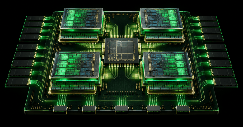
FUJITSU-MONAKA is a 144-core Arm server processor scheduled for 2027. Fujitsu’s official architecture material shows a 3D chiplet design with 2 nm core dies stacked over separate 5 nm SRAM dies, plus a 5 nm I/O die, 12 DDR5 memory channels, PCI Express 6.0, and CXL 3.0 support.
The most unusual part is the cache hierarchy. Fujitsu says the entire last-level cache sits on the separate SRAM dies beneath the compute dies rather than consuming valuable area on the 2 nm core silicon.
Tom’s Hardware highlighted that architecture in an August 26 X post from Hot Chips 2026, where Fujitsu also disclosed that MONAKA uses 256-bit SVE2 vector execution and is targeting 350 W and 500 W server configurations.
Why Waste 2 nm Silicon on SRAM?
Leading-edge logic nodes are valuable because they can pack high-performance transistors more densely and improve performance per watt. But SRAM does not scale as cleanly as logic from one node to the next, and large caches can consume a huge fraction of a modern CPU die.
Fujitsu’s answer is to separate those jobs physically. The processor cores use 2 nm technology, while the last-level cache is built on 5 nm SRAM dies. Fujitsu says the 2 nm portion accounts for less than 30% of the total die area in the package.
That means the most expensive process node is concentrated on the logic that benefits most from it instead of being used to manufacture large blocks of cache that can remain efficient on a more mature node.
This is a different partitioning philosophy from BitcoinVersus.Tech’s recent look at NUVACORE’s Core First processor strategy. NUVACORE is trying to delay the ISA decision while keeping the microarchitecture reusable. Fujitsu is using physical partitioning to decide which parts of the CPU deserve the newest manufacturing node.
The Cache Is Separate, but It Still Has to Feel Local
Moving the cache off the compute die only works if the connection between the two remains fast enough that cores do not constantly pay a large latency penalty.
Fujitsu uses a tightly coupled 3D structure with through-silicon vias between the 2 nm core dies and the 5 nm SRAM dies underneath. The goal is to make the off-die cache behave much more like a nearby extension of the core than a conventional external memory device.
Tom’s Hardware’s Hot Chips analysis describes four compute-die and SRAM-die pairs around a central I/O die, all tied together through the package and silicon interposer.
MONAKA Uses 144 Arm Cores Without SMT
MONAKA is designed around 144 Armv9.3-A cores per socket and up to two sockets per node, giving a 288-core server configuration.
The design is aimed at cloud, AI, and HPC workloads where throughput, power efficiency, memory bandwidth, and predictable server behavior matter more than simply chasing desktop-style peak frequency.
That puts MONAKA in a different class of Arm infrastructure than the processors that first made Arm popular. BitcoinVersus.Tech recently covered SiPearl’s Rhea1 entering the JUPITER supercomputer, another example of Arm moving deep into HPC and data-center systems once dominated by x86 and specialized architectures.
Why Fujitsu Narrowed the Vector Width
MONAKA also makes an interesting vector-design tradeoff. Fujitsu’s earlier A64FX processor used 512-bit SVE vectors. MONAKA moves to SVE2 with 256-bit execution units.
A narrower vector path does not automatically mean a slower processor. Wider vectors consume die area and power, and they only help when software can keep those lanes busy. A server CPU aimed at cloud, AI orchestration, general HPC, and mixed workloads may benefit more from a balanced design with more cores, more efficient execution, and strong memory throughput.
That makes MONAKA’s 256-bit SVE2 decision a useful reminder that architecture is not a checklist where every larger number is automatically better. The right width depends on workload mix, power budget, compiler behavior, and how much silicon the design can justify dedicating to vector hardware.
Twelve DDR5 Channels Keep the Cores Fed
A 144-core server processor creates enormous pressure on the memory subsystem. Fujitsu pairs MONAKA with 12 DDR5 channels, which is critical because adding cores without enough memory bandwidth simply creates more processors waiting for data.
The central 5 nm I/O die handles the external interfaces while the compute and cache stacks remain focused on execution and local data access. That separation again reflects the same architectural philosophy: build each function on the process node and physical structure best suited to it.
IBM is approaching the CPU problem from a completely different direction with its new dual-ISA Arm and z/Architecture core. Together, the two designs show how diverse server CPU architecture has become: one vendor is rethinking the ISA boundary, while another is rethinking where the cache physically lives.
Chiplets Are Becoming About Economics as Much as Performance
Chiplets are often discussed as a way to increase core counts or build processors larger than a single monolithic die. MONAKA shows another reason to split a CPU: different parts of the processor have different manufacturing economics.
The cores benefit from the densest, most power-efficient logic process. SRAM may not. I/O transistors have their own voltage, analog, and reliability requirements. Separating those blocks lets Fujitsu avoid paying leading-edge-node costs for every square millimeter of the package.
The tradeoff is packaging complexity. More dies mean more bonding, more interfaces, more thermal interactions, more validation, and more ways for manufacturing yield to become a systems problem rather than a single-die problem.
The CPU Package Is Becoming the Architecture
MONAKA is a good example of how modern processor design is moving beyond the old idea that the CPU is one piece of silicon.
The compute dies, SRAM dies, I/O die, interposer, DDR5 interfaces, PCIe/CXL links, cooling system, and software-visible Arm architecture all have to work together as one processor.
That makes packaging decisions architectural decisions. Cache latency depends on die stacking. Cost depends on node allocation. Memory performance depends on the I/O die. Thermals depend on how heat moves through vertically integrated silicon.
Fujitsu is betting that the right server CPU is not simply the one with the newest node everywhere. It is the one that uses the newest node only where it produces the most value.
Editor’s Note
We volunteer daily to ensure the credibility of the information on this platform is Verifiably True. If you would like to support our research initiatives, please donate here: 3C9o19EH5HSiwEPyCTmEKzxhNCbo2X6TTb
BitcoinVersus.tech is not a financial advisor. This media platform reports on financial subjects purely for informational purposes.


Leave a Reply