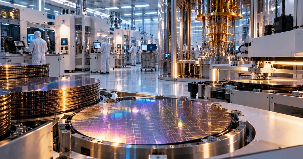
IBM-backed Anderon is no longer just a plan for a quantum-chip factory. The company says its first quantum wafers are already moving through a 300-millimeter production facility in Albany, New York.
On September 16, 2026, Anderon finalized a $1 billion CHIPS and Science Act award from the U.S. Department of Commerce. IBM is backing the foundry with an additional $1 billion investment, bringing the announced public-and-private commitment to roughly $2 billion.
IBM CEO Arvind Krishna introduced Anderon earlier in 2026 as a purpose-built quantum chip foundry intended to serve a broad range of companies.
A Foundry for Quantum Chips, Not Just IBM
The interesting part is the business model. Anderon describes itself as a pure-play quantum foundry: customers design quantum hardware, while Anderon handles wafer fabrication. That is structurally closer to the merchant-foundry model used in classical semiconductors than to a research lab that only builds chips for its own machines.
The company’s September announcement says the Albany facility is intended to fabricate quantum wafers for customers across the ecosystem. It starts with superconducting qubit arrays, quantum input/output structures and readout signal-chain components, with plans to support additional quantum modalities later.
IBM Research’s official Anderon introduction explains the foundry model and why IBM believes quantum manufacturing has to move beyond bespoke laboratory fabrication.
Why 300mm Matters
Three hundred millimeters is the standard wafer diameter used throughout much of advanced semiconductor manufacturing. Larger wafers allow more dies to be processed at once and support highly automated tooling, tighter process control and around-the-clock manufacturing.
IBM moved its newer quantum processors onto 300mm manufacturing at the NY CREATES Albany NanoTech Complex before Anderon was spun out. In a 2025 technical overview, IBM said Loon, Nighthawk and future roadmap chips were being fabricated on 300mm tooling because the older 200mm research-style process was too bespoke and too slow for the scale it wants to reach.
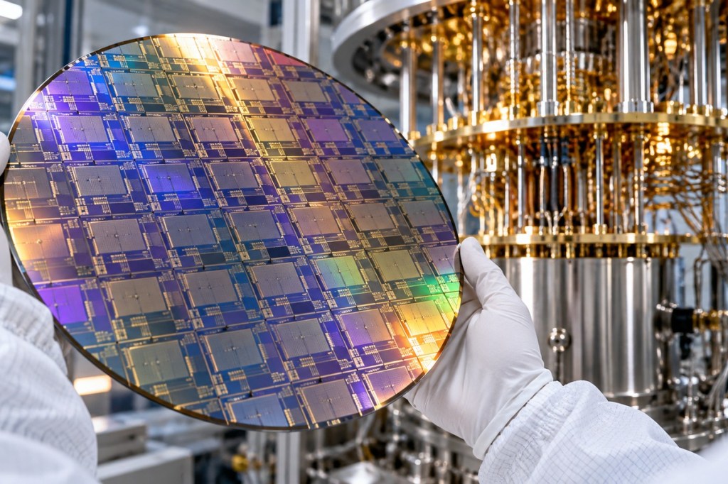
This does not mean quantum chips are suddenly manufactured exactly like CPUs or GPUs. Superconducting qubits depend on specialized metals, junctions, microwave structures, packaging and extremely low-temperature operation. The advantage is that more of the fabrication discipline can now be borrowed from mature semiconductor production.
The First Wafers Are Already in Process
The biggest update in the September agreement is operational: Anderon says its first quantum wafers are already running through the manufacturing facility. That moves the project beyond a funding commitment or construction roadmap.
The company has not publicly disclosed a full customer list, commercial wafer volumes or production yields. Those details will matter if Anderon is going to prove that a neutral quantum foundry can work economically outside IBM’s own roadmap.
That uncertainty matters because BitcoinVersus has already documented that the quantum industry still has no single winning hardware architecture. Superconducting qubits, trapped ions, neutral atoms, photonics and semiconductor spin qubits all impose different manufacturing demands.
Loon Shows What the Foundry Is Building Toward
IBM Quantum Loon is one example of the kind of processor enabled by this manufacturing shift. Loon is a prototype designed around fault-tolerant computing research, with 112 qubits and long-range couplers intended to support newer error-correcting code layouts.
IBM Research’s Loon demonstration shows one of the quantum processor families fabricated using the company’s newer 300mm manufacturing approach.
The challenge is not simply fitting more qubits onto a wafer. Manufacturing has to produce junctions, couplers and interconnects consistently enough that entire systems can be calibrated and operated with useful error rates.
This Is Becoming a Foundry Race
Anderon is not alone in trying to industrialize quantum-chip fabrication. BitcoinVersus recently covered SkyWater’s merchant quantum foundry effort, which supports multiple quantum technologies through established semiconductor manufacturing infrastructure.
Photonic quantum computing is taking another route. Xanadu and GlobalFoundries are moving photonic quantum chips toward higher-volume manufacturing, using silicon-photonics processes rather than superconducting qubit wafers.
The emerging competition is therefore not just “which company has the most qubits?” It is increasingly about which architectures can be manufactured repeatedly, packaged, interconnected and scaled without custom handwork at every generation.
A Quantum Version of the Foundry Model
Calling Anderon the “TSMC of quantum” would be premature. TSMC operates at enormous commercial volume with a mature global customer base, while quantum computing is still early and fragmented.
But the underlying idea is similar: separate chip design from the expensive manufacturing infrastructure required to build the hardware. If that model works, a quantum startup would not need to create its own leading-edge fabrication line before testing a new processor architecture.
IEEE Spectrum’s recent look at Anderon emphasizes the same manufacturing bottleneck: quantum companies can invent new qubits faster than they can necessarily build them repeatably at production scale.
What Is Confirmed
- Anderon is an IBM company headquartered in Albany, New York.
- It operates a production-scale 300mm quantum wafer foundry.
- The U.S. Department of Commerce finalized a $1 billion CHIPS award for Anderon in September 2026.
- IBM is contributing an additional $1 billion investment.
- Anderon says its first quantum wafers are already running through the facility.
- The initial manufacturing focus includes superconducting qubit arrays, quantum I/O and readout-chain components.
- The foundry is intended to serve outside quantum companies, not only IBM.
- Commercial customer scale, wafer volumes and long-term yields have not yet been publicly demonstrated.
The larger shift is easy to miss. Quantum computing is starting to develop the same industrial layers that classical semiconductors built decades ago: design companies, fabrication specialists, packaging, tooling and supply chains. Whether useful fault-tolerant machines arrive on IBM’s timetable is still uncertain. But quantum-chip manufacturing is becoming a real industry before that question is settled.
BitcoinVersus.Tech
Editor’s Note: Anderon’s descriptions of its capabilities and first wafers are company-reported. A functioning 300mm foundry does not by itself prove that any quantum architecture has reached commercial-scale fault-tolerant computing.
We volunteer daily to improve the credibility of the information on this platform. If you would like to support the research, please donate here: 3C9o19EH5HSiwEPyCTmEKzxhNCbo2X6TTb
BitcoinVersus.tech is not a financial advisor. This media platform reports on technical and financial subjects purely for informational purposes.


Leave a Reply