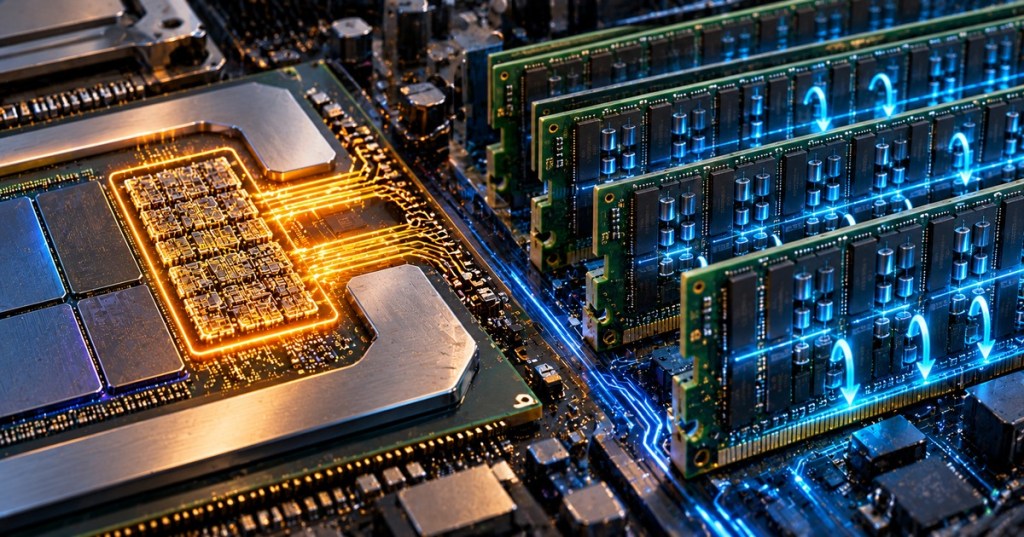
SRAM and DRAM are both volatile semiconductor memory, but they are optimized for very different jobs. SRAM is built for speed and predictable access. DRAM is built for density and capacity. That difference is why processors use relatively small amounts of SRAM for cache while computers use much larger amounts of DRAM for main memory.
The simplest distinction is architectural: SRAM stores a bit in a small latch made from several transistors, while DRAM stores a bit as electrical charge in a capacitor controlled by a transistor. The SRAM cell takes more silicon area but can be accessed quickly without a refresh cycle. The DRAM cell is much smaller and cheaper per bit, but its charge leaks and must be refreshed periodically.
| Category | SRAM | DRAM |
|---|---|---|
| Full name | Static Random Access Memory | Dynamic Random Access Memory |
| Typical cell | Commonly 6 transistors | Commonly 1 transistor + 1 capacitor |
| Refresh required | No, while powered | Yes |
| Latency | Very low | Higher |
| Density | Lower | Higher |
| Cost per bit | High | Low |
| Common use | CPU/GPU cache, buffers, embedded memory | System RAM, HBM, GDDR, LPDDR |
How SRAM Stores a Bit
Static RAM usually stores each bit in a bistable circuit made from cross-coupled transistors. A common six-transistor SRAM cell uses four transistors to hold the state and two access transistors to connect the cell to the bit lines during reads and writes.
Because the state is maintained by active transistor feedback, the cell does not need the periodic refresh operation required by DRAM. As long as power remains applied, the latch keeps its value. That helps SRAM deliver low and relatively deterministic access latency.
Infineon’s SRAM documentation highlights this lack of refresh overhead and the resulting deterministic access behavior. That characteristic is useful not only in processor caches but also in networking, industrial control, automotive, aerospace and other systems where worst-case memory latency matters.
How DRAM Stores a Bit
Dynamic RAM is optimized around a much smaller cell. A conventional DRAM cell uses one access transistor and one capacitor. The capacitor represents the stored state by holding electrical charge, while the transistor connects the cell to a bit line when the memory controller accesses it.
The trade-off is leakage. Capacitors cannot retain their charge indefinitely, so the memory system must periodically refresh the array. Reads are also destructive at the cell level: sensing the tiny charge changes the stored state, so the data must be restored after it is read.
That sounds inefficient compared with SRAM, but the tiny 1T1C structure is the reason DRAM can pack enormous amounts of memory into a practical area and price. Micron’s DRAM portfolio spans DDR5, DDR4 and legacy products, while related DRAM technologies such as LPDDR, GDDR and HBM adapt the same basic density advantage to mobile, graphics and high-performance computing.
Why SRAM Is Faster
SRAM does not need row activation, charge sensing, restore and refresh in the same way DRAM does. Its cell state can be read directly through transistor logic, and SRAM arrays can be built physically close to processor execution units. That combination is why SRAM is widely used for L1, L2 and L3 caches.
Physical distance matters too. An L1 cache sitting beside a CPU core can be reached far more quickly than an external DIMM across a memory controller and motherboard traces. The advantage therefore comes from both the memory technology itself and where the memory sits in the system.
Why DRAM Is Denser
The six-transistor SRAM cell consumes far more silicon area than a one-transistor, one-capacitor DRAM cell. If a manufacturer tried to build a normal 64 GB system-memory module entirely from SRAM, the die area and cost would be prohibitive compared with DRAM.
DRAM therefore wins where capacity matters. Modern systems can install tens or hundreds of gigabytes of DDR memory because the cell is dense enough to manufacture economically. In servers and AI accelerators, stacked DRAM becomes high-bandwidth memory, trading more complex packaging for far greater aggregate bandwidth.
Cache vs Main Memory
The SRAM-versus-DRAM trade-off creates the modern memory hierarchy. Processor registers are extremely small and fast. SRAM cache sits beneath them in progressively larger L1, L2 and L3 levels. DRAM sits farther away as main memory, providing far more capacity at higher latency. Storage sits below that again, providing still more capacity but much longer access times.
The cache system works because most programs repeatedly touch a smaller working set of instructions and data. If the requested data is already in SRAM cache, the processor avoids waiting for DRAM. When the cache misses, the system fetches a larger block from main memory and places it in cache in anticipation of future reuse.
Latency Is Not Just One Number
Memory speed is frequently reduced to a clock rate, but real latency depends on several steps. DRAM access may involve opening a row, waiting for sensing, selecting a column, transferring data and eventually closing or changing rows. A row hit can be much faster than an access that requires a different bank or row state.
SRAM has its own timing constraints, but its simpler access path makes it far better suited to caches that must respond within a small number of processor cycles. This is why comparing DDR data rate directly with CPU cache frequency does not tell the full performance story.
Power Is More Complicated Than It Looks
DRAM consumes energy refreshing cells even when useful application data is not being transferred. SRAM avoids refresh, but a large SRAM array can consume significant leakage and occupies much more transistor area. That means neither technology is automatically “lower power” in every system.
The useful metric is energy for the amount of useful data delivered under the intended workload. Designers choose SRAM when avoiding latency and repeated external memory traffic saves more energy than the SRAM itself costs. They choose DRAM when capacity and density dominate.
SRAM Inside CPUs and GPUs
Modern CPUs dedicate substantial die area to SRAM caches because arithmetic units are useless when they are starved for data. GPUs also contain large amounts of on-chip SRAM in caches, shared memory, register files and buffers even though their highest-capacity memory is external GDDR or HBM.
This same balance explains the heterogeneous processor systems in our CPU vs GPU vs NPU vs TPU comparison. Different processors organize their local SRAM differently, but every high-performance architecture is trying to reduce expensive trips to larger external memory.
DRAM Is Not Storage
Both SRAM and DRAM are volatile: remove power and the stored data disappears. NAND flash is different. It is nonvolatile and can retain data without power, which makes it suitable for SSDs. Our guide to NAND, SSD controllers and DRAM cache shows how storage systems often combine nonvolatile flash with faster volatile memory for metadata and buffering.
Which One Wins?
- Lowest latency: SRAM.
- Highest density: DRAM.
- Lowest cost per bit: DRAM.
- No refresh requirement: SRAM.
- CPU and GPU cache: SRAM.
- Main system memory: DRAM.
- Best real system: both, arranged as a hierarchy.
Bottom Line
SRAM and DRAM are not competing replacements for one another. SRAM spends silicon area to buy speed. DRAM accepts refresh and higher latency to buy density. The entire modern memory hierarchy exists because computers need both: small pools of extremely fast memory close to computation and much larger pools of affordable memory behind them.
BitcoinVersus.Tech Editor’s Note:
We volunteer daily to ensure the credibility of the information on this platform is Verifiably True. If you would like to support to help further secure the integrity of our research initiatives, please donate using the QR code provided

For best QR-code scanning results, please scan this donation code from a desktop or larger screen. Mobile screens may prevent camera recognition.


Leave a Reply